Resolve The Stress Caused By High-Speed Interfaces
June 4, 2013
7 min read
This file type includes high resolution graphics and schematics.
The race to embrace new high-speed interfaces like USB 3.0, DisplayPort 1.2, and PCI Express 3.0 has created tremendous stress for electronics OEMs around the world. The increase in data rates introduces challenging signal integrity issues of a magnitude that digital designers have never had to face before.
It’s not that these new interfaces are impossible to implement. Rather, engineers have much less error margin to work with. Attenuation, jitter, and impedance become even more important to handle carefully. If these factors are too pronounced, interface reliability suffers in ways that can directly impact the user experience through digital media quality degradation, substantially reduced throughput, and even loss of data.
Attenuation
The farther and faster a signal has to travel through a system, the more it will degrade. For example, the attenuation losses of an interface operating at 2.5 Gbits/s are commonly on the order of 0.3 dB per inch of FR4 printed-circuit board (PCB) trace. Moving to a next-generation interface operating at 8 Gbits/s brings attenuation up to 0.9 dB, nearly tripling the losses.
Related Articles
- Optimize Timing Margins For Your High-Speed Interface
- High-Speed Interfaces Provide Design Flexibility
- Signal-Conditioner ICs Extend High-Speed Interfaces While Lowering Costs
As a consequence, high-speed interface standards typically require the receiver and transmitter to be placed right next to the interface connector to minimize trace length. With the many interfaces today’s complex systems need to support, however, physically accommodating this requirement isn’t always possible.
Consider an average notebook with high-speed video connectors (HDMI or Display Port), a high-speed USB 3.0 connector, PCI Express slots, and possibly a Thunderbolt connector. To fit all of the I/O connectors on a single platform, a designer isn’t going to be able to easily lay out each high-speed transmitter next to its paired connector. Certain transmitters then will need to drive multiple inches of trace with possible vias until the signal finally reaches its paired connector. The same issue arises with highly integrated processors supporting multiple interfaces whose pinouts may not match the placement of the physical interface connectors on the board.
Jitter
Several forms of jitter impact signal integrity. Deterministic jitter arises from differing transition rates within the data signal. As high-speed interfaces have more variation along the data stream, engineers must deal with greater jitter. A primary source of random jitter is a noisy source clock. The host processor or an external clock source generates this clock, and it runs concurrently with the data signal.
Ideally, the clock signal is as accurate as possible, and many technologies can provide the required accuracy. However, the chip sourcing the clock may be difficult to place next to the interface transceiver. For example, when the host processor sources the clock, the interface transceiver must compete with all of the other subsystems to be near the host while still being close to the interface connector. When the clock signal has to run long distances, more noise can couple onto the signal and introduce random jitter unless there is good isolation, along the clock path. In addition, if impedance mismatching occurs, clock signal quality degrades even faster.
Impedance
Impedance matching uses PCB ground layers to provide signal isolation and prevent high-speed signals in a system from coupling with each other. High signal losses from attenuation and jitter mean more isolation will be required. A high-speed signal with high jitter might require a 10-layer PCB compared to the same signal with low jitter requiring only a six-layer PCB.
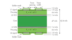
Figure 1 shows the nominal four-layer PCB stack-up that can be used to carry high-speed PCI Express signals when signal conditioning is applied to both transmit and receive signals. In addition, no new PCB technology is required since the system can handle the attenuation losses inherent in FR4-based PCBs. Thus, failure to effectively address attenuation and jitter can significantly increase system cost.
Signal Integrity
Reducing effective trace length can mitigate attenuation. Rather than a signal having to span the entire distance between the transmitter and receiver (which, for external interfaces, includes at least two connectors and a cable as well as all board traces), the signal gets a “rest” on the way, so to speak.
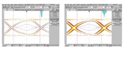
Redriving restores the signal to its full integrity by receiving it and then retransmitting it. When the signal is restored in this way, deterministic jitter can be eliminated through equalization and preemphasis techniques that anticipate losses and correct for them (Fig. 2). The integrity of clock signals can be recovered in this way as well to reduce random jitter.
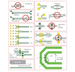
Signals can be redriven in a very small space, on the order of 4 by 4 mm, which can be placed close to the interface connector. For systems with a host processor with multiple interfaces, this gives engineers more flexibility in host processor and interface connector placement since redriving extends the maximum distance a signal can be transmitted reliably. Signal integrity can be further improved by strictly adhering to best practices for trace layout and routing (Fig. 3).
Consider a plasma screen connected using HDMI to an inexpensive DVD player with a noisy power source. Unless the plasma screen can compensate for the low-quality signal coming from the DVD player, the picture quality will be poor. Consumers may also associate the poor quality with the screen rather than the player. While they would be mistaken, it would still have a major negative impact on their perception of the screen OEM’s brand value.
To prevent this, designers can utilize an equalizer to clean up incoming signals. The same redriver (repeater) that restores a signal for transmission can recover signal integrity for signals that are received. Restoring the signal quality in this way ensures that systems will work reliably regardless of the quality of the devices to which they are connected.
Signal losses are a part of high-speed interface design, and they can make compliance with minimum interface requirements difficult. By maintaining signal integrity throughout the signal path and redriving the signal to restore signal integrity before transmitting and when receiving a signal, engineers can ensure reliable operation of their products while protecting brand value.
Abdullah Raouf is a senior product marketing manager for Pericom Semiconductor. With a BSEE from the University of California Davis, he has worked for over 10 years in business development and product marketing, mainly focusing on the semiconductor industry. He also serves as a member of the VESA, HDMI, and USB organizations.
Joseph Juan is a product marketing manager for Pericom Semiconductor.
This file type includes high resolution graphics and schematics.
About the Author
Abdullah Raouf
Senior Product Marketing Manager
Abdullah Raouf is a senior product marketing manager for Pericom Semiconductor. With a BSEE from the University of California Davis, he has worked for over 10 years in business development and product marketing, mainly focusing on the semiconductor industry. He also serves as a member of the VESA, HDMI, and USB organizations.
Joseph Juan
Product Marketing Manager
Joseph Juan is a product marketing manager for Pericom Semiconductor.
Sign up for our eNewsletters
Get the latest news and updates


