Software and instruments chase blazingly fast signals
High-speed digital technology invokes many disciplines, ranging from design and simulation software to interconnect and on to test and compliance. Companies including ANSYS, Cadence Design Systems, Keysight Technologies, National Instruments, Tektronix, and Molex have weighed in on the design, simulation, test, and interconnect challenges imposed by demands for ever-lower cost, but ever-more-capable tech products.
High-speed digital challenges begin with design. “Our customers are facing the daunting task of designing reliable high-speed serial links in the double-digit gigabit-per-second rates with decreasing power-supply voltages and design margins while requiring extremely low bit-error rates (BER) of 10-12 in some applications,” said Ken Willis, product engineering architect in the Custom IC and PCB Group at Cadence Design Systems. “Our solution allows customers to design, model, and emulate their hardware and optimize their equalizer settings to achieve the best-possible signal quality for their particular channel.”
Addressing challenges ahead in 2018, Willis added, “We are seeing data rates increasing, power-supply voltages decreasing, voltage and timing margins tighten, more adoption of multilevel signaling like PAM4, and use of complex adaptive equalizers being implemented in high-speed digital communications.”
Complexity imposes challenges for high-speed design, test, and measurement. “Our customers are faced with rapidly changing technology and increased complexity in validating their designs,” said David Njuguna, technical marketing manager at Tektronix. “This complexity can come from additional test coverage or convergence of multiple technologies on a design.” He added that customers require solutions that let them focus on validating their device—not on being test-equipment experts. “Tektronix solutions provide turnkey automation for simplified validation at the same time they provide the ability to drill deep to debug complex issues—for example, the training of a PCI Express or Ethernet link,” he said.
Looking ahead, Njuguna said, “We expect to see the deployment of new technology being driven by new industry consortiums including 100G Lambda MSA, CCIX, and Gen-Z. The industry is moving fast, and we expect to see more application-specific selection of technology. We also expect coherent optical to grow into new applications as the cost to deploy the technology is reduced.”
Brig Asay, director of strategic planning, Internet Infrastructure Group, Keysight Technologies, cited consumer demands as driving key trends in high-speed-digital design and test and the role of PAM4 in addressing these trends. “Consumers are demanding faster and yet more compact products that serve their evolving needs,” he said. “Higher data rates such as the new 100G and 400G Ethernet infrastructures require much more efficient modulation techniques, and PAM4 fulfills this requirement. Having leading-edge test equipment in the signal-integrity lab that can measure PAM4 provides the competitive edge now required.”
Asay also cited power-integrity issues, noting that effective high-speed designs require resonance-free power-distribution networks. “EMI is a large issue, and most EMI stems from poor PI design,” he said. “High-density routing in PCBs creates non-ideal ground planes (perforated with holes), which in turn increases resistance and voltage drops (IR drop) on power planes.” He added that high data rates create more signal processing, resulting in more heat in the board that increases voltage drop and reduces reliability. The company offers an electrothermal simulation solution within its PiPro tool that provides a complete solution for the PI workflow (Figure 1).
Courtesy of Keysight Technologies
Cost-of-test is a key focus for National Instruments. “As more lower-cost devices have serial interfaces that must be tested, lower-priced instrumentation with sufficient capabilities for testing these devices must emerge,” said Michael Keane, product marketing engineering, test systems, at NI. “By using protocol-aware instrumentation, test engineers can perform protocol functional tests to quickly and affordably verify a SerDes interface. With the addition of user-programmable FPGAs in test instruments becoming more popular, users will be able to further customize their instruments to meet their exact application needs such as in-line data processing or closed-loop control.”
Keane sees a lack of protocol-aware test solutions for custom serial interfaces. “The user-programmable FPGA and openness of NI’s high-speed serial instruments allow engineers to integrate their custom IP into the test instrument to test their custom interfaces,” he said. “Furthermore, many customers have benefited from the flexibility of the instrument to interface to different high-speed serial interfaces by simply flashing a new bitfile. This enables a single instrument to test different serial interfaces on the same or different DUTs, allowing for flexible and scalable test systems.”
High-speed connectivity
A critical component to any high-speed-digital design is the interconnect that carries the high-speed data. “Customers designing and manufacturing high-speed equipment and networks rely on seamless connectivity for network, server, and storage devices to ensure the rapid and efficient flow of data,” said Bratislav Kostic, new-product development manager for backplanes at Molex. “As more infrastructure moves to the cloud, network equipment must support faster processing, more bandwidth, and increased density, with optimal signal integrity.” He added, “Increasingly, customers seeking ways to avoid using traditional printed-circuit boards are turning to hybrid layouts in order to control costs.”
He continued, “As data volume and speeds increase, degraded signal-integrity performance becomes an issue for network equipment design engineers. Additionally, they need scalability to minimize future infrastructure investments.”
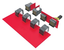
One Molex approach to meeting the challenges is the Impulse orthogonal direct backplane connector system (Figure 2). Kostic said the forward-compatible Impulse system supports 56- or 112-Gb/s (NRZ and PAM4, respectively) data rates, making it suitable for switches, routers, and other high-density applications. The Impulse system eliminates the need for a mid-plane structure, thereby boosting signal integrity and improving airflow and thermal management—all at a lower applied cost. “The innovative signal interface improves insertion loss over traditional beams, pushing interface resonance well beyond 35 GHz,” he said.
Courtesy of Molex
“Those designing switches, routers, and servers need I/O and backplane connections capable of high bandwidth speeds and efficiency, with excellent signal integrity and thermal management in densely packed circuits,” Kostic continued. “Designed for high-speed connections, Molex BiPass I/O and backplane cable assemblies provide a low-insertion-loss alternative to PCB traces. BiPass assemblies meet 56- and 112-Gb/s PAM4 protocol. They feature terminated I/O ports connected via twinax to high-density connectors to dramatically reduce signal-to-noise ratios from the ASIC to the I/O. The integrated, one-piece design with board-mount connectors ensures easy installation in data-communications, telecom, and networking applications,” he concluded.
From SI to electrothermal behavior
Mark Ravenstahl, technical director, strategic partnerships and business development at ANSYS, identified several trends for 2018. “The key trends in high-speed digital design will continue to be the drive toward greater speed, smaller size, and greater functionality,” he said. “These trends directly lead to signal-integrity, power-integrity, EMI, and thermal-design concerns.”
Ravenstahl commented on some specific application areas. “Designing advanced driver-assistance systems [as well as] IoT, 5G, and other high-performance digital systems demands simulation technology well beyond a good circuit-simulation tool,” he said. To that end, the company offers its ANSYS Chip-Package-System (CPS) design flow, which enables customers to maximize power efficiency and accurately predict signal-integrity, power-integrity, EMI, and electrothermal behavior. “ANSYS CPS allows circuit and system analysis to be part of the broader 3D electromagnetic assembly solution rather than the other way around,” Ravenstahl said. “With ANSYS CPS you can ‘assemble’ an electronic system with IC packages, printed-circuit boards, connectors, and cables just as you would in the real world, then perform analysis of that system using appropriate technology.”
He continued, “With electronic systems evolving at a rapid pace, chip designs become increasingly complex, even for mundane tasks. In most design environments, ICs work within the context of a reference system that the IC vendor provides as a guide to the system designer. The challenge for system designers is meeting these guidelines and managing design specifications (performance) and margins (price) while addressing the demands of a rapidly changing market.”
He emphasized that the CPS development methodology is multiscale, multiphysics, and multiuser. “The methodology is multiscale, in that it provides simulation technologies that range from the nanometer scale, used in IC and other chip designs, to the meter scale, found in servers, unmanned aerial vehicles, and other designs,” he said. “Multiphysics gives developers the ability to simulate various physical phenomena across chips, packages, and systems, including power optimization, signal integrity, ESD, EMI/EMC, heat transfer, fluid dynamics, and structural mechanics.”
Finally, he said, “The multiuser aspect provides the simulation platform and collaboration tools that enable electronics, electrical, and mechanical engineers—along with managers and executives from different divisions within the organization—to collaborate in designing increasingly complex products.”
Ravenstahl said the CPS methodology provides simulation tools that span a large variation in scale while incorporating a variety of components and subsystems into a single simulation, thereby enabling engineers to simulate and optimize signal and power integrity (SI/PI) for the entire CPS channel as a single system, rather than a collection of parts and components.
He also addressed thermal integrity and structural reliability. “ANSYS is the only provider that offers a design flow spanning electrical, thermal, and mechanical analysis,” he said. “Structural and thermal integrity are critical design considerations for packages/PCBs that affect reliability and product lifecycle.”
He called thermal impact on the package, especially the IC, a key driver for material-selection, cooling, and form-factor decisions that ultimately determine the size, weight, and cost of the final product. “It is critical for package and system designers to determine the thermal signature of their system,” he said. “ANSYS provides automated thermal analysis from SIwave that streamlines EM-thermal-coupled analysis and links to ANSYS Mechanical for analysis of the structural impact on the electronic package.”
Finally, he addressed ANSYS 3D Layout Assembly with 3D Components. “One of the most common challenges in performing complex system simulations is data sharing with IP protection, simulating large 3D models, and creating a schematic entry to wire models from different field solvers to better predict system time- and frequency-domain performance,” he said. “These challenges are resolved via ANSYS 3D Layout Assembly with ANSYS 3D Components.” He described 3D Components as a self-contained HFSS tool that may contain an assembly of model geometry, excitations, boundary conditions, and parametric variables. “3D Layout with integrated HFSS offers a layout assembly approach for connecting PCBs, ICs, and arbitrary 3D components,” he said.
Test products
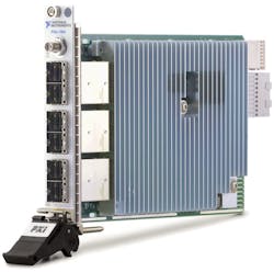
Recently introduced test products for high-speed digital applications include NI’s PXIe-7902 high-speed serial instrument (Figure 3), which features six Mini-SAS HD (Molex iPass+ HD) connectors supporting rates up to 12.5 Gb/s. Each connector includes four AC-coupled, differential Tx and Rx channels for a total of 24. “Though designed for Serial-Attached SCSI (SAS), these connectors work with a variety of serial protocols and offer very high density,” said NI’s Keane. “With the power of an open, user-programmable FPGA, the card offers the flexibility of testing both standard and custom serial interfaces. NI’s high-speed serial instruments excel at protocol-aware test and lightweight characterization applications in which price and fast measurement times are key concerns.”
Courtesy of National Instruments
Keane noted that many protocols have different application-layer variations, which make them difficult to address with standard, fixed-hardware test instruments. “For example, companies that deploy base stations and small cells into the communication infrastructure around the world commonly use the CPRI protocol as a foundation and then add custom IP and algorithms on top of that protocol,” he said. “We developed our high-speed serial instruments to be software-designed, giving users out-of-the-box functionality for base protocols with the ability to add their own algorithms to the FPGA fabric, using LabVIEW FPGA or Xilinx Vivado.”
DesignCon 2018
DesignCon 2018, scheduled for Jan. 30 to Feb. 1 in Santa Clara, CA, will give ANSYS, Cadence, Keysight, Molex, NI, Tektronix, and other exhibitors the opportunity to highlight their products for high-speed digital applications.
The CPS and structural and thermal integrity design flows will be the focus of the ANSYS exhibit, Ravenstahl said, explaining that the CPS design flow uses advanced modeling and proven simulator technologies to enable an intelligent, integrated, chip-aware system design flow to solve power integrity, signal integrity, EMI/EMC, ESD, and thermal stress challenges. “ANSYS will demonstrate our unique layout assembly capability to integrate IC package layout, interposers, connectors, ribbon cables, flex cables, and PCB layout all within a single assembly,” he added.
The company’s structural and thermal integrity design flow addresses critical design considerations for packages and PCBs that affect reliability and product lifecycle. “Thermal impact on the package, especially from the IC, is a key driver for material selection, cooling, and form-factor decisions that ultimately determine the size, weight, and cost of the final product,” he said. “It is critical for package and system designers to determine the thermal signature of their system.”
ANSYS will also feature new automated thermal analysis—part of SIwave—that streamlines EM-thermal-coupled analysis and links to ANSYS Mechanical for analysis of the structural impact on the electronic package. In addition, Ravenstahl said, ANSYS will demonstrate HFSS, Icepak, and RedHawk at DesignCon.
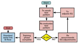
For its part, Cadence will be exhibiting the Sigrity SystemSI with backchannel capability (Figure 4). “Cadence is presenting the industry’s first IBIS-compliant backchannel support,” said Willis. “This capability helps high-speed digital communication customers achieve optimum signal quality by enabling the receiver to automatically adjust transmitter equalization settings through a ‘backchannel’ to produce the best eye-diagram possible for their particular channel.”
Courtesy of Cadence Design Systems
Test and measurement
Keysight is serving as the event’s host sponsor and has scheduled demonstrations related to memory, signal integrity, data analytics, and power integrity. Specific standards and formats that Keysight will address include PAM4, PCI Express Gen4, USB Type-C, and MIPI Gear 4/UFS 3. With regard to this last, Asay said, “MIPI Alliance has released the new M-PHY v4.1 specification for the industry’s fastest mobile chip-to-chip communication, and Keysight, at the frontier of the MIPI test solution, will show industry’s first M-PHY Gear4 PHY layer testing.” The demonstration will make use of a DSAV334A Infiniium V-Series oscilloscope, MIPI M-PHY compliance test software, and an M8020A J-BERT high-performance BERT.
In addition, Keysight will demonstrate its Physical Layer Test System (PLTS) 2017, which has new capabilities with regard to manufacturing test of high-speed interconnects, such as cables, backplanes, PCBs, and connectors, Asay said. “The emergence of advanced, high-data-rate channels introduced the problem of how Tx/Rx chip IP developers and system designers could concurrently and independently proceed with their product implementations,” he said. “A new facet to standardization was needed, to define how analysis of these channels could be pursued.” This led to the definition of the Channel Operating Margin methodology. “This is a complex MATLAB script implemented within PLTS that is user-definable for flexibility,” he explained. “Again, PLTS successfully takes a very complex test methodology and implements a user-friendly interface to simplify testing for the signal-integrity engineer.” In addition to the PLTS software, the demonstration will make use of a E5071C vector network analyzer.
Yet another demonstration related to signal integrity will embrace simulation and data analytics. “This demo will showcase the latest enhancements in Keysight EEsof ADS 2017 for signal-integrity channel simulations and the latest release of Keysight’s data-analytics software for collating, slicing, and analyzing measured and simulated data,” Asay said. “The new Interconnect Toolbox in ADS adds parameterized-via-design capability for quickly generating optimal via designs accurate to high-frequencies.”
Datacenter emphasis
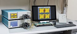
Tektronix plans to exhibit its products that enable next-generation datacenters, according to Njuguna. “Our solutions are focused on the R&D and manufacturing markets for optical and electrical networking, and the server/storage market,” he said. Specific products on display will likely include DPO77002SX ATI performance oscilloscopes capturing PAM4 plots (Figure 5).
Courtesy of Tektronix
“One of the key pain points that our customers face is seamless deployment of their technology from R&D to manufacturing,” he said. “The shift to PAM4 signaling technology has added complexity to the validation process during the R&D phase. Tektronix recently introduced new optical test solutions that leverage both the real-time and sampling platforms, enabling our customers with the right solution at the right time within their test workflow.”
Njuguna continued, “Within the server/storage space, customers are quickly moving to the next generations of interconnects,” including the shift to new interfaces such as CCIX and Gen-Z in addition to the next generation of PCI Express, which will run at 32 Gb/s NRZ. “Tektronix is well positioned with solutions today to address these emerging standards,” he concluded.
Embracing time and frequency domains
Other DesignCon exhibitors have not disclosed their plans for the show as of press time in early December. But a look at recent news from prospective DesignCon exhibitors, such as Rohde & Schwarz, suggests what they might feature. At productronica last November, for example, Rohde & Schwarz highlighted solutions for 5G, IoT, and automotive applications. For instance, the R&S SMW200A vector signal generator and the R&S FSW43 signal and spectrum analyzer combine to support Verizon 5GTF signals and numerous 5G candidate waveforms in the frequency range up to 40 GHz. For M2M and IoT applications, the company highlighted the R&S CMW290 functional radio communication tester, suitable for measuring the transmitter and receiver characteristics of an NB-IoT module or chipset. The company also highlighted oscilloscopes to facilitate the development of associated embedded designs, analysis of integrated power electronics, or troubleshooting.
Bottom line—whereas high-speed time-domain measurements may once have been relegated to shows like DesignCon and frequency-domain measurements relegated to the International Microwave Symposium, modern design and test requires expertise in both domains. Refer to the online version of this article for updates as the event nears.
For more information:
About the Author

Rick Nelson
Contributing Editor
Rick is currently Contributing Technical Editor. He was Executive Editor for EE in 2011-2018. Previously he served on several publications, including EDN and Vision Systems Design, and has received awards for signed editorials from the American Society of Business Publication Editors. He began as a design engineer at General Electric and Litton Industries and earned a BSEE degree from Penn State.


