What’s the Difference Between OpenCAPI, CXL, and Gen-Z?
For designers of data centers and their components, dealing with massive amounts of data presents enormous challenges, one of which is transmitting data efficiently between memory and processors such as CPUs, SoCs, and GPUs. Fortunately, promising new standards and approaches have been developed to improve the processor’s local near-memory domain access as well as provide fabric-attached far-memory domain access.
The Open Coherent Accelerator Processor Interface (OpenCAPI) and its Open Memory Interface (OMI) subset, in addition to the Compute Express Link (CXL), deliver new capabilities and performance levels to address near-memory domain bottlenecks. Meanwhile, Gen-Z is focused on rack and data-center scale far-memory domain challenges.
Near and Far Memory
The two memory domains have similar challenges but address them differently. The near-memory domain, for example, is where memory is local to the processor, typically mounted on a parallel DDR DIMM (double-data-rate dual in-line memory module). Far-memory delivers shareable pools of memory resources to servers that increase system memory utilization and improve application performance, as arrays of processors can simultaneously operate on a shared memory pool.
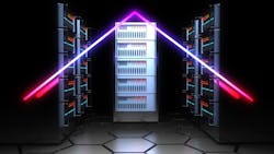
There are three areas of improvement for near-memory. The first is to increase the number of processor memory channels and their available bandwidth by using far fewer pins on the processor (Fig. 1). The second is to provide media independence so that system builders can optimize their designs by using whatever media makes the most sense for a set of cost and performance requirements. And the third is to lower the cost of the processor memory subsystem itself.
Far-memory innovation is focused on providing processors with low latency load/store access to data stored in a shared memory pool. Traditional approaches move the data from a remote block storage device into the processor’s locally attached memory for processing and then writing the results back to the remote block storage device—introducing significant latency.
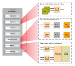
In fact, some systems use more than half their energy moving data between the processor and the remote block storage infrastructure. Gen-Z provides a secure and resilient fabric interconnect (Fig. 2) so that processors can directly operate on the data in the shared memory pool without moving it. This effectively moves data closer to the processor and minimizes the need for costly data movement.
Far-memory provides a host of additional benefits, including dynamic memory capacity scaling through disaggregation, separate technology scaling between processors and memory, enablement of high-availability architectures resulting from separate fault domains for far-memory, increased memory utilization, and high-performance data sharing among processors. However, far-memory also has some limitations and barriers to adoption, such as higher latency, lack of “guaranteed” cache coherence, and the significant investment required in software infrastructure. These will surely be dealt with as the concept becomes more precisely defined and deployed.
Far-memory is very appealing because, in the future, data centers will utilize vast memory pools initially deployed at the rack level but increasingly scaled for sharing between thousands of physical machines and hardware accelerators. Processors will share the same coherent and non-coherent memory spaces as the capabilities of far-memory infrastructure develop and as applications require it.
The Memory Conundrum
Computers have developed over the years to form a divide between computation performed in processors and accelerators on one side, and block data storage and the rest of the system on the other. As a result, there’s a massive amount of data movement before computation can be performed. This consumes lots of power and has high latency, so a considerable portion of a system’s energy is spent moving data rather than computation.
Furthermore, the amount of data produced by data-intensive applications is rapidly increasing while these applications are simultaneously demanding computation at extremely high speeds. The result is a significant memory bottleneck that’s worsening, as efficiently scaling memory capacity and bandwidth becomes more difficult, especially for DRAM. Consequently, it’s become essential to minimize data movement and reduce its impact on system performance.
In short, the performance of direct-attached memory hasn’t kept pace with the compute, and that’s hindering application performance. The processor’s performance can be only as high as the efficiency of the path between the CPU and DRAM. If this continues, execution time would increasingly depend on the speed and latency of memory transfers rather than the performance of the processor itself, and cores in higher-core-count processors would themselves become underutilized resources.
Parallel Problems
The industry’s long-standing reliance on parallel communication between memory and processor has also become a major performance impediment. As the number of processing cores rises within CPUs it decreases the average memory bandwidth available to each processing core. This is because CPU and SoC devices can’t scale the number of parallel DDR interfaces on a single chip to meet the needs of increasing core operating frequency and core count.
The trend over the last 15 years has been to replace parallel interfaces with serial interfaces, in which the buses transferring data operate on serial rather than parallel streams. Today, almost all interfaces are already serialized, from the SRAM and flash to mass storage. However, DRAM continues to communicate with processors using single-ended, parallel connections that have reached the limit of what can be delivered in a reasonable amount of space, cost, and power.
The current standard, DDR4, has replaced DDR3 in most applications thanks to its lower supply voltage and higher speed. Its successor, DDR5, still retains a parallel interface, but it’s showing signs of hitting cost and performance limits. To achieve higher bandwidth, DDR5 is resorting to a larger quantity of error-correcting-code (ECC) bits to do the same task as DDR4—a waste of DRAM capacity. DDR5 also requires a larger number of bank groups than DDR4, adding design complexity to the processor.
Serial Solutions?
An increasingly appealing answer to this conundrum is serial-attached near-memory, which has significant benefits compared to its parallel counterpart but has historically been considered too slow for CPU-attached memory applications. That is, its incremental latency—the time required to convert data from a parallel to a serial stream, transit it through the serial link, and convert it back into parallel data—has been too long compared to a native parallel interface. CPUs are now deploying native serial-attached memory interfaces to gain access to these benefits.
While this incremental latency is unacceptable for some applications, advances in silicon technology have reduced it to significantly lower levels. The trend toward serial memory interfaces has been championed by IBM and members of the OpenCAPI Consortium that defined the Open Memory Interface (OMI)—the memory semantics portion of OpenCAPI. Most major CPU manufacturers have publicly backed this trend with the recent announcement of IBM, Arm, AMD, and Intel supporting the recently launched CXL Consortium.
As proof of the performance advantages of this technology trend, consider that IBM’s Power9 Advanced I/O (AIO) processors, which the company unabashedly calls the “bandwidth beasts,” have abandoned all parallel DRAM interfaces in favor of up to 16 OMI 3.1 memory interfaces. IBM’s flagship processors achieved a memory bandwidth increase from Power9’s standard parallel DDR 200 GB/s to the Power9 AIO’s blistering 600 GB/s along with a major boost in memory capacity (Fig. 3). The latency penalty is an astonishingly low 5 to 10 ns, according to IBM, which it deems sufficient for the moment.
The Near-Memory Serial Contenders
The OpenCAPI and Open Memory Interface (OMI)
OpenCAPI was initiated by IBM, AMD, Google, Mellanox, and Micron, and is now in its fourth generation. OpenCAPI, which allows CPUs to attach point-to-point to accelerators, I/O devices, and advanced memories, is agnostic to processor architecture. It’s well-suited for computing supported by accelerators with minimal accelerator overhead. Attached devices operate natively within an application and coherently with processors; therefore, devices participate in applications without kernel involvement. Along with its 32-Gb/s signaling bandwidth, version 4.0 also supports 4, 8, and 16 lanes along with cache coherence.
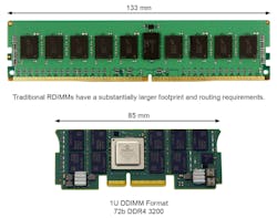
Of course, OMI (and the other standards) require a serial memory controller to support them and Microchip Technology is first out of the gate with a solution with its SMC1000 8x25G (Fig. 4) launched in August 2019. The device is designed to exploit the capabilities of OMI while adding some Microchip features as well. The SMC1000 8x25G supports three DDR4 data rates, DDR4-2666, DDR4-2933, and DDR4-3200. It provides an eight-lane OMI 3.1 interface to the CPU or SoC with ECC and support for four ranks of memory – all within a power efficient 1.7W. The product achieves three key values of serial attached near-memory – higher system bandwidth performance, media independence, and lower cost memory subsystem cost. Partner companies – Samsung, SmartModular, and Micron have all released initial 84-pin, 85 mm DDIMM modules that are far more pin and space efficient than the 288-pin, 133 mm standard DIMM memory modules.
Compute Express Link (CXL)
CXL is an open interconnect standard founded by Alibaba, Cisco, Dell EMC, Facebook, Google, HPE, Huawei, Intel, and Microsoft. The consortium has grown rapidly to more than 70 members in a few short months and, as noted, now includes all major CPU manufacturers and leading GPU suppliers like Nvidia and AMD.
The initial CXL 1.1 standard release supports a rich set of point-to-point capabilities that provide a window directly into the processor caching hierarchy. This extends the low latency load/store domain outside of the DRAM memory subsystem for the first time to support a wide array of heterogeneous computing elements from CPUs to GPUs, FPGAs, smart NICs, AI devices, and other accelerator components.
CXL is pin-multiplexed with PCIe Gen5 in order to support the smooth transition of thousands of products now supporting the ubiquitous PCIe standard. Utilizing the same PCIe Gen5 physical layer and operating at a rate of 32 GT/s, CXL supports dynamic multiplexing between its three sub-protocols—I/O (CXL.io based on PCIe), caching (CXL.cache), and memory (CXL.memory).
The CXL.io protocol is used for device discovery, configuration, initialization, I/O virtualization, and direct memory access (DMA), a superset of today’s PCIe standard. CXL.cache enables attached devices to interoperate with the CPU caches so that devices can own, operate on, and return coherent memory. CXL.mem enables memory expansion so that CXL attached memory appears seamlessly alongside the rest of the CPU’s memory resources. It remains to be seen whether CXL will expand beyond its current point-to-point capabilities to support fabrics as PCIe does today.
Gen-Z, the Far-Memory Solution
Gen-Z is a memory-semantic fabric founded by AMD, ARM, Broadcom, Cray, Dell EMC, Hewlett Packard Enterprise (HPE), Huawei, IDT, Micron, Samsung, SK Hynix, and Xilinx—and has rapidly expanded to more than 70 member companies. By unifying the communication paths and simplifying software through load/store memory semantics, Gen-Z allows many types of devices to work together. It’s the best defined and robust consortium specification for supporting far-memory and accelerator applications.
Gen-Z supports signaling rates of 16, 25, 28, and 56 GT/s (and later 112 GT/s) for both PCIe and 802.3 Ethernet electrical standards to ensure its longevity while tuning each of its communication paths to different workloads. Gen-Z also supports up to 64-way memory interleaving across a set of point-to-point or switched attached memory components and offers hardware-enforced isolation and integrated security along with support for almost all routing algorithms.
Rather than closely coupling memory to processors, Gen-Z decouples it, placing media-specific functionality with the media itself. This allows every processor in the system to be media agnostic, so that each device can scale independently from others. As all devices are peers and speak the same memory-semantic language, a system can scale with diverse processing, memory, and storage resources independently.
Summary
Major advances in memory infrastructure are being developed to meet the challenges of scaling memory bandwidth and availability to meet the demands of data-hungry applications. OpenCAPI, CXL, and Gen-Z are poised to solve many of the problems associated with parallel memory bus structures. And with the support of the biggest players’ high-performance computing, there’s lots of momentum and energy going into solving these complex problems. While they will surely evolve, one thing is certain: The trend toward serial memory interfaces is here to stay.
Jay Bennett is Sr. Manager, Product Marketing, Data Center and Solutions business unit at Microchip Technology.
About the Author
Jay Bennett
Sr. Manager, Product Marketing, Data Center and Solutions business unit, Microchip Technology
Comment About the Article
To join the conversation, and become an exclusive member of Electronic Design, create an account today!

Leaders relevant to this article: