What’s the Difference Going from PCIe 3.0 to PCIe 6.0?

Download this article in PDF format.
The Peripheral Component Interconnect (PCI) architecture has provided I/O connectivity for computing, communication, and storage platforms for more than three decades. From its inception as a local bus interface for all types of I/O devices in the PC industry, it has evolved as a point-to-point link-based interface (PCI Express) to satisfy the I/O requirements across the cloud, enterprise, artificial intelligence, PC, embedded, IoT, automotive, and mobile market segments.
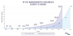
This is made possible due to the ability of PCI Express (PCIe) architecture to seamlessly deliver cost-effective, HVM (high-volume manufacturing) friendly, power-efficient, high-bandwidth, and low-latency solutions through six generations of technology evolution, doubling the data rate in every generation (Fig. 1) while maintaining full backwards compatibility with all prior generations to protect customer investments.
One salient and unique feature of the PCIe specification is that while it supports multiple data rates and multiple widths to back the different performance needs of different devices across a wide range of usage models, they interoperate with each other. This enables both silicon and platform developers to design and validate to one specification. Even though a multitude of form factors (e.g., M.2, U.2, CEM, various flavors of SFF) have evolved to meet the needs of diverse systems across the compute continuum, they all use the same silicon ingredients based on a common PCIe base specification.
The success of PCI technology as a ubiquitous I/O interconnect is due to it being an open industry standard, backed by a robust compliance program to ensure seamless interoperability between devices from different companies. PCI-SIG, a consortium of more than 800 member companies, spread across the globe, owns and manages PCI specifications and runs the compliance program. PCI-SIG expects PCIe technology to continue to evolve to meet the diverse I/O needs across the entire compute continuum for many more years to come.
This article delves into the details of PCIe technology covering its evolution from the fourth through the sixth generation, as a follow-up to our prior article in Electronic Design covering the first three generations.
The First Three PCIe Generations at 2.5, 5.0, and 8.0 GT/s
PCIe technology started off in 2003 at a 2.5-GT/s data rate, supporting widths of x1, x2, x4, x8, and x16 for different bandwidth levels. The supported widths haven’t changed through the six generations of evolution of PCIe architecture. PCIe 2.0 specification doubled the data rate to 5.0 GT/s in 2006. The first two generations of PCIe technology used 8b/10b encoding, incurring a 25% encoding overhead. This was needed to establish dc balance and for the additional encodings required for physical-layer packetization (e.g., to indicate start and end of different types of packets) and training handshake.
In terms of the PCIe 3.0 specification, a strategic decision was made to increase the data rate to 8.0 GT/s instead of 10.0 GT/s. This was augmented with a new 128b/130b encoding mechanism to double the bandwidth per pin over PCIe 2.0 (1.6 due to data-rate increase × 1.23 with the encoding overhead reduction). The new encoding mechanism ensured high reliability by adopting a fault model of three random bit flip detections and had several innovative approaches to perform physical-layer framing of packets while preserving the packet format delivered from the upper layers (Link and Transaction).
The decision not to double the data rate (to 10.0 GT/s) was made with data from extensive analysis to ensure that PCIe 3.0 can work on existing channels with the projected silicon and platform ingredient capabilities of the time of the specification’s introduction (2010) and still meet projected power and cost constraints. Backchannel equalization was introduced in PCIe 3.0 specification to mitigate the effects of channel loss on the platform by silicon ingredients. The encoding and equalization mechanisms of PCIe 3.0 architecture was robust enough to sustain subsequent generations of speed increases.
In addition to greater speed, PCIe’s evolution during this time supported features such as I/O virtualization and device sharing to accommodate the emerging trend of supporting multiple independent virtual machines and containers in a single platform. To support the performance needs of accelerators, it added features such as caching hints, atomics, and lower-latency accesses through enhanced transaction bypass semantics.
To help with the evolution of handheld segments such as smartphones and tablets, we enhanced our low-power states with deeper low-power states. This enabled devices to maintain their states for a quicker resumption of traffic while consuming power in the single digits of microwatts. This mechanism for lower power consumption during idle state along with the industry-leading power efficiency during active state (around 5 pJ/bit), plus a fast transition time between the two (1 to 100 µs), results in PCIe architecture being the interconnect of choice across low-power as well as high-performance segments.
October 2017: PCIe 4.0 Specification at 16.0 GT/s
The journey to double the data rate from 8.0 GT/s to 16.0 GT/s took longer to ensure that platform and silicon ingredients could evolve in a cost-effective and power-efficient manner for a seamless technology transition. The channel loss budget was increased to 28 dB. The routing material continued to get better with newer and economically feasible materials such as Megtron-2 (4, and 6) with improved loss characteristics, along with improvements in packaging technology, making it feasible within the cost and power constraints of platforms with hundreds of lanes.
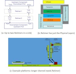
Even then, though, it wasn’t enough to cover longer channel lengths such as 20 in. with two connectors. With board materials used in systems and available packaging technology, we can support about 15 in. of board trace with one connector and an add-in card. Retimers had to be formally specified as channel-extension devices. Retimers have the full physical layer and double the channel loss. Up to two retimers are allowed in a link, enabling longer-reach channels with PCIe architecture (Fig. 2).
PCIe 4.0 technology allowed more outstanding transactions to sustain the ever-increasing bandwidth capabilities through scaled flow-control credit mechanisms and extended tags. It also enhanced the reliability, availability, and serviceability (RAS) features to enable migration to direct-connected PCIe storage devices through downstream port containment. Furthermore, systems can run non-destructive lane-margining capabilities without interrupting the system operation. As always, these enhancements will sustain a few generations of bandwidth increases.
A question naturally arises, though: How did the systems deal with the I/O bandwidth needs when the technology transition from PCIe 3.0 to PCIe 4.0 specification took longer than usual due to the inflection points that had to be addressed? The answer is nuanced.
Platforms that debuted with PCIe 3.0 architecture had about 40 lanes of PCIe technology coming out of every CPU socket. Just prior to the transition to PCIe 4.0 specification, the lane count per CPU socket increased dramatically, reaching up to 128 lanes per CPU socket in some platforms. Thus, while the per-slot (e.g., x16) bandwidth didn’t increase, the aggregate I/O bandwidth increased 3X in platforms, both in terms of the number of lanes as well as measured I/O bandwidth.
Storage tends to be an aggregate bandwidth driver, with each storage device connected to the system using a narrow link (e.g., x2 or x4). Thus, increasing storage needs were met with lane count increase. Networking is a single-slot usage; during this time, it transitioned from 10 Gb/s to 100 Gb/s and dual 100-Gb/s network interface cards (NICs). This bandwidth was accommodated by NICs moving from x4 to x16 (and 2 x16 for dual 100-Gb/s NICs) width—a great tradeoff from a power/cost/performance perspective. Accelerators and GPGPUs also evolved to make efficient data moves through proper transaction sizing and protocol hints.
Overall, the slowdown in speed evolution from PCIe 3.0 to PCIe 4.0 architecture was mitigated by a width increase, thanks to the flexibility offered by PCIe specification. The ecosystem evolved naturally, so the speed transition was accomplished in a cost-effective and power-efficient manner.
May 2019: PCIe 5.0 Specification at 32.0 GT/s
The past few years have seen a significant change in the computing landscape as cloud computing, edge computing, and applications such as artificial intelligence, machine learning, and analytics have led the demand for faster processing and movement of data. As the compute and memory capability increases at an exponential pace, we need to sustain I/O bandwidth doubling at an accelerated cadence to keep up with the performance of emerging applications.
For example, 400 Gb (or dual 200 Gb) networking needs a x16 PCIe at 32.0 GT/s to sustain the bandwidth. This required the release of a fully backwards compatible PCIe 5.0 in less than two years after PCIe 4.0 architecture—a significant achievement for a standard.
The evolution from PCIe 4.0 to PCIe 5.0 specification was primarily a speed upgrade. The 128b/130b encoding, which was the protocol support to scale bandwidth to higher data rates, was already built in with PCIe 3.0 and PCIe 4.0 specification. The channel loss was extended to 36 dB along with enhancements to the connector to minimize the loss with the increased frequency range. With the improvement in board material and packaging technologies, the channel reach is like PCIe 4.0 technology, using retimers to extend the channel reach.
One of the enhancements made with PCIe 5.0 architecture is the built-in support for alternate protocols. As PCIe technology has evolved to be the highest bandwidth, most power-efficient, and most widely deployed interface, some usages require additional protocols, such as coherency and memory to run on the same pins as PCIe architecture. For example, certain accelerators and smart NICs may cache the system memory and map their memory to system memory space for efficient data exchange and atomics in addition to PCIe protocols. Similarly, system memory is migrating to PCIe PHY due to the power-efficient high bandwidth and low latency solution it offers.
Other protocols are employed, too, such as symmetric cache coherency between components using PCIe PHY. Support for alternate protocols on PCIe PHY is provided to meet these user requirements, preventing the fragmentation of the ecosystem with different PHY for different usages.
Targeted for 2021 Release: PCIe 6.0 Specification at 64 GT/s
We continue the accelerated journey to double the bandwidth again in two years in a backwards-compatible manner. Applications such as AI, machine learning, gaming, visual computing, storage, and networking continue to demand bandwidth increases as we find ourselves in a virtuous cycle of more throughput driving new applications with greater capabilities.
Devices such as GPUs, accelerators, high-end networking (800 Gb/s), coherent interconnects, and memory expanders continue to demand more bandwidth at an accelerated pace. Constricted form-factor applications that can’t boost width also demand increased frequency to deliver performance.
There are significant challenges to doubling the data rate beyond 32.0 GT/s using the NRZ (non-return-to-zero; i.e., the binary signaling where a 0 or a 1 is transmitted in every unit interval, or UI) method due to the channel loss. Thus, PCIe 6.0 will adopt PAM4 (pulse amplitude modulation, 4-level) signaling (Fig. 3), which has been widely adopted by networking standards when they moved to data rates of 56 Gb/s and beyond. Using this method, two bits are encoded using four levels in the same UI, allowing PCIe 6.0 UI (and Nyquist frequency) to be identical to PCIe 5.0 architecture.

While PAM4 alleviates the channel loss due to running at half the frequency with two bits per UI, it’s more susceptible to errors due to various noise sources caused by reduced voltage (and timing) ranges. This manifests as a higher bit error rate (BER), several orders of magnitude higher than the 10-12 BER for PCIe 1.0 through PCIe 5.0 specifications.
Another side effect is the correlation of errors due to correlated error sources such as power-supply noise as well as error propagation in the same lane due to the decision feedback equalizer (DFE). These effects are mitigated by deploying a forward-error-correction (FEC) mechanism, which has the drawback of reduced link efficiency due to the FEC bits as well as the latency add for the encoding/decoding mechanisms. The stronger the FEC, the worse the performance characteristics. However, the effective bit error rate improves due to correction.
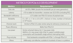
For example, some of the existing standards have a 11% bandwidth loss and a FEC latency of greater than 100 ns, which don’t meet the bandwidth and latency demands of a load-store interconnect like PCIe technology. PCIe 6.0 specification development is following the guardrails in terms of key metrics delineated in the table below. While these are challenging goals and haven’t been solved before, we must meet these metrics to ensure that PCIe continues to be a high-performance interconnect.
With FEC, we need a fixed FLIT (flow control unit) size to apply the correction. With a fixed FLIT size, it’s advantageous to have the error-detection mechanism (cyclic redundancy check, or CRC) operate on the FLIT. Since PCIe defines the data-link-layer packet (DLLP) and transaction-layer packet (TLP) of variable sizes, we define the payload to align to FLITs. Thus, a FLIT can have multiple DLLPs and TLPs, and a TLP/DLLP may span across multiple FLITs.
In this new mode, since the FLIT includes the CRC, the DLLP and TLP will not carry their individual CRC bytes as they did in prior generations. Furthermore, since FLITs are fixed size, there’s no need to have a PHY layer framing token (4 bytes) for every TLP or DLLP. These savings help improve efficiency to overcome the FEC overhead.
The packet efficiency with PCIe 6.0 architecture exceeds that of prior generations for payloads up to 512 bytes. For example, a 4DW (Double Word, each double word is 4 bytes) request TLP will have a TLP efficiency of 0.92 with FLIT-based encoding versus 0.62 in prior generations (with 128b/130b encoding and a 5% DLLP overhead). This results in an ~3X improvement in effective throughput (2X from data rate increase and ~1.5X improvement in TLP efficiency). As the TLP size increases, efficiency drops; for the 4-kB data payload size, it reduces to 0.98, in line with the bandwidth inefficiency provided in the metrics provided in the table. An example FLIT layout is shown in Figure 4.
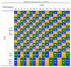
Figure 5 demonstrates the tradeoffs associated with the raw burst error rate on a wire (error propagation to multiple bits is considered as one error) and the effectiveness of different FEC to handle that error. A single symbol error-correcting code (ECC) corrects one error burst, whereas a double symbol ECC corrects up to two error bursts.
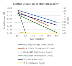
While the length of the burst follows a certain probability distribution function, the ECC code is defined such that the probability of a burst exceeding the ECC capability is negligible. Simulations and silicon data have been used to make the tradeoff between the error rate, the nature of the burst, the channel constraints, and the silicon capability. PCIe 6.0 is targeting a burst error probability of 10-6, which will result in a retry probability of the FLIT of around 10-6.
Since PCIe has a low-latency link-level retry mechanism, we don’t need to deploy a strong FEC, which will increase the latency and bandwidth overhead. A retry probability of 10-6 (or even 10-5) is a reasonable tradeoff, resulting in the FEC latency adder of 1-2 ns in each direction. In the case of a retry (a 10-6 probability event), the FLIT is delayed by ~100 ns due to the round-trip retry mechanism. This is a reasonable tradeoff versus adding 100+ ns to every FLIT with a strong FEC and paying a high bandwidth penalty. Details of the PCIe 6.0 specification are available to members from the PCI-SIG website.
Conclusion
With a rich and successful history of navigating several technology transitions in a backwards-compatible manner spanning three decades, PCI-SIG is well-positioned to continue leading the changing computing landscape going forward. The power and promise of this open standards organization, backed by the combined innovation capability of 800+ member companies, makes our technology nimble, scalable, cost-effective, power-efficient, leading-edge, and multi-generational, with relevance across all market segments and usage models for the foreseeable future.
Dr. Debendra Das Sharma is a PCI-SIG Board Member and an Intel Fellow at Intel Corp.
About the Author

Debendra Das Sharma
PCI-SIG Board Member, UCIe Consortium Chair, and Intel Fellow, Intel Corp.
Dr. Debendra Das Sharma is an Intel Fellow and Director of I/O Technology and Standards Group. He is an expert in IO subsystem and interface architecture, delivering Intel-wide critical interconnect technologies in Peripheral Component Interconnect Express (PCIe), coherency, multichip package interconnect, SoC, and rack scale architecture. He has been a lead contributor to multiple generations of PCI Express since its inception, a board member of PCI-SIG, and leads the PHY Logical group in PCI-SIG. He also is chair of the UCIe Consortium.
Debendra joined Intel in 2001 from HP. He has a Ph.D. in Computer Engineering from the University of Massachusetts, Amherst and a Bachelor of Technology (Hons) degree in Computer Science and Engineering from the Indian Institute of Technology, Kharagpur. He holds 99 U.S. patents. Debendra currently lives in Saratoga, Calif. with his wife and two sons. He enjoys reading and participating in various outdoor and volunteering activities with his family.
Comment About the Article
To join the conversation, and become an exclusive member of Electronic Design, create an account today!

Leaders relevant to this article: