Standard CMOS Yields Integrated Photonic 100-Gb/s Optical Modulator

Due to materials realities and device physics, it’s challenging to develop high-performance optical transceiver functions on standard CMOS processes, but the potential benefits of such photonic integration are substantial. Now, a team at the Optoelectronics Research Centre (ORC) of the University of Southampton (UK) has demonstrated an all-silicon photonics transmitter can operate at over 100 Gb/s with on/off keying (OOK).
They accomplished the feat by using an innovative design for the electrical CMOS driver, which overcomes the limited-bandwidth dilemma of other silicon-based photonic modulators. They maintain that this achieved performance represents a doubling of speed compared to existing research efforts.
Their approach optimizes the tradeoff among the different performance metrics: high bandwidth, low optical-insertion loss, low drive voltage, low fabrication cost, small device footprint, and device reliability while achieving the speed and bit-error-rate (BER) goals. The team initially looked at using inductive peaking, a standard technique for bandwidth enhancement in high-speed electrical circuit designs.
Instead, though, they selected “T-coil” peaking using an asymmetrical transformer that can provide an additional 70% bandwidth enhancement in broadband amplifier designs. The PN doping levels of the silicon modulator were increased so that the modulation efficiency was enhanced, leading to optimization of the electrical-power efficiency and photonic-device footprint.
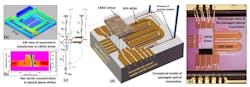
The optical modulator is configured as a U-shaped Mach-Zehnder modulator (MZM) designed and modeled for operation at a wavelength of 1550 nm, a physical arrangement that provides access to both input and termination pads of the MZM via one side of the chip (Fig. 1). This allows both ends of the modulator to be electrically connected to the CMOS driver by flip-bonding.
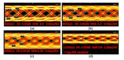
To test the device, they multiplexed two lower-rate 27 − 1 pseudorandom bit sequences (PRBS) to create a bit stream at up to 112 Gb/s with a single-ended voltage swing of approximately 0.5 V, and fed this signal into the driver amplifier. The optical output from the modulator was amplified by a low-loss erbium-doped fiber amplifier (EDFA) and then fed into a digital communication analyzer.
The test circuit voltage rail was 2.8 V, and the overall power consumption of the CMOS driver was 203 mW plus an additional 20 to 35 mW for the heating element, which sets operating point on the silicon modulator. The optical eye diagrams at 56, 80, and 100 Gb/s (all with OOK) show the integrated silicon photonics transmitter operating with an approximately 3-dB extinction ratio and a power efficiency of 2.03 picojoules (pJ)/bit even above 100 Gb/s OOK (Fig. 2).
Dr, Ke Li, lead author and lead inventor on the technology's associated patents, says: "In contrast to previous work in the field, we have introduced a new design philosophy where photonics and electronics must be considered as a single integrated system in order to tackle the demanding technical challenges of this field."
Professor Graham Reed, Deputy Director of the ORC, adds, "Our results are based upon a fully integrated electronic-photonic system, not a laboratory probed standalone silicon modulator. In all other work to date that does not rely on digital signal processing to recover signal integrity, integration of the electronics and photonics has resulted in an inferior system performance as compared to the performance of the individual components, resulting in a maximum data rate of approximately 56 Gb/s.” He goes on to say, "At a time when most researchers around the world are striving for a system-level improvement of the order of 5% to 10%, our results represent close to a 100% improvement.”
The silicon modulator was fabricated through Southampton’s own research fabrication foundry service, then integrated with the custom modulator drivers that were designed in-house and fabricated at TSMC (28-nm high-K-metal-gate process), followed by fabrication and integration work done at the university’s cleanroom complex. Details are in their brief paper “Electronic–photonic convergence for silicon photonics transmitters beyond 100 Gbps on–off keying,” which is published in the OSA’s lead journal Optica as both an HTML page and available as a downloadable PDF document.
About the Author

Bill Schweber
Contributing Editor
Bill Schweber is an electronics engineer who has written three textbooks on electronic communications systems, as well as hundreds of technical articles, opinion columns, and product features. In past roles, he worked as a technical website manager for multiple topic-specific sites for EE Times, as well as both the Executive Editor and Analog Editor at EDN.
At Analog Devices Inc., Bill was in marketing communications (public relations). As a result, he has been on both sides of the technical PR function, presenting company products, stories, and messages to the media and also as the recipient of these.
Prior to the MarCom role at Analog, Bill was associate editor of their respected technical journal and worked in their product marketing and applications engineering groups. Before those roles, he was at Instron Corp., doing hands-on analog- and power-circuit design and systems integration for materials-testing machine controls.
Bill has an MSEE (Univ. of Mass) and BSEE (Columbia Univ.), is a Registered Professional Engineer, and holds an Advanced Class amateur radio license. He has also planned, written, and presented online courses on a variety of engineering topics, including MOSFET basics, ADC selection, and driving LEDs.
Comment About the Article
To join the conversation, and become an exclusive member of Electronic Design, create an account today!

Leaders relevant to this article: