Programmable THz-Wave Beamforming Surface Built from CMOS Tile Array
What you'll learn:
- How researchers created metasurfaces for THz signal distribution that don't have the typical drawbacks of similar structures.
- How the tile arrays are laid out to form the metasurface.
- What do the meta-elements used in the design consist of?
The terahertz spectrum—generally considered as the span from 100 GHz (3-mm wavelength) or even 300 GHz (1 mm) up to 3 THz (100 µm) or even 10 THz (30 µm)—offers great potential due to its enormous bandwidth and unique electromagnetic proprieties. But it’s a difficult zone in the spectrum for creating real systems, as it lies in the gap between the better-understood, high-gigahertz RF range and the very different optical world.
However, that hasn’t stopped researchers and, in fact, has encouraged them, as demonstrated by a team at Princeton University. They developed a way to use “metasurfaces” to implement control of both space and time of the far-field and near-field distribution of terahertz signals. This capability is useful to applications such as high-speed wireless communication, high-resolution imaging, and sensing. (Metasurfaces are two-dimensional surfaces with precisely designed scatterers that create controlled field transformation of amplitude, phase, frequency, and polarization properties of incident wavefronts.)
Their approach has demonstrated the ability to create and use metasurfaces to control fundamental electrical and magnetic material properties and thereby the overall surface impedance. As a result, they’re able to manipulate electromagnetic (EM) wave propagation.
In contrast to conventional optical or antenna design, these surfaces are designed with carefully engineered scattering structures at sub-wavelength scales to collectively provide abrupt phase and amplitude changes of the incident terahertz field. The design using flat metasurfaces provides scattering structures capable of a desired EM transformation.
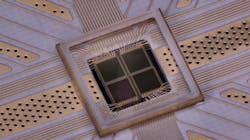
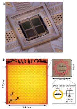
To accomplish this, the team created a programmable terahertz metasurface with fully integrated silicon chip tiles, fabricated using an industry-standard 65-nm CMOS process. Each such chip holds an array of 12×12 elements, with each element individually addressable and programmable with 8-bit control. Next, they created a 2×2 array of these tiles, yielding a two-dimensional surface with a total of 576 meta-elements (122×22) that are independently digitally reconfigurable at a maximum clock speed of 5 GHz (Fig. 1).
1. Dynamically programmable and scalable THz metasurface with tiled silicon chips: a) Perspective and top view of the fabricated 2×2 tiled metasurface chips operating at 0.3 THz. b) A single silicon chip tile measuring 2×2 mm2 overall, fabricated in an industry-standard 65-nm CMOS process, consists of a programmable 2D array of 12×12 meta-elements. (Source: Princeton University)
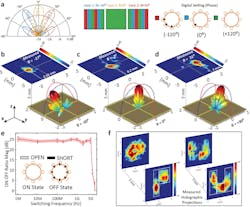
They were able to demonstrate that the programmable surface offered amplitude modulation with a switching depth of 25 dB, operation as a spatial light modulator, reconfigurable beamforming of ±30° via phase-controlled surfaces, and programmable holographic projections at 0.3 THz (Fig. 2). They also feel that their tile-based approach is scalable to even larger arrays and potentially to the adjacent spectral regions.
2. Programmable THz beamforming, high-speed switching for spatial light modulation, and dynamic holographic projections: a) Simulated beamforming due to linear phase gradients along one axis of the metasurface. A group of four unit-cells is consecutively set to a particular digital setting to achieve a specific linear phase gradient. b-d) Simulated and measured beamforming at −30°, 0° , and +30° respectively at 0.3 THz. The measurements demonstrate close correspondence with simulation. e) Measured ON-OFF ratio of the transmitted wave across the metasurface for the two digital states (all open and all short) as the clock frequency is varied from 1 MHz to 8 GHz. The measured amplitude depth modulation is about ∼25 dB up to 5 GHz, enabling high-speed spatial light modulation. f) Measured near fields and holographic projections of letters “P” and “U,” respectively, at a distance of 5 mm. (Source: Princeton University)
They note that this isn’t the first THz-regime metasurface, but existing approaches have drawbacks as their reconfigurability requires phase-change materials that rely on temperature gradients, microelectromechanical systems (MEMS), two-dimensional materials, phase-change materials, and metal oxides (all of these approaches are referenced via published citations called out at the end of their paper).
Those approaches typically have slow response time, require large external stimuli (heat, optical pumping, or high voltages) and don’t offer the potential to scale; some also require cryogenic operating temperatures. Instead, what’s desired is a topology that enables complex EM transformations for scalable metasurfaces with individually addressable elements, simultaneous amplitude and phase control, and gigahertz-rate reconfiguration.
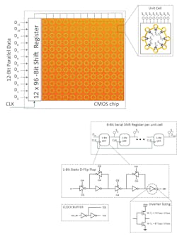
In contrast, the Princeton team was able to create active meta-element structures by incorporating passive meta-element multiple active devices within each subwavelength, all strongly coupled with deeper subwavelength inductive loops. Their terahertz elements are each less than 100 µm in diameter and 3.4 µm high, made of layers of copper and coupled with active electronics that collectively resonate with the structure (Fig. 3).
3. The CMOS metasurface integrated chip architecture. The control signal for each meta-element/unit cell is provided through an 8-bit shift register. (The sizing of these transistors is also shown.) One metasurface tile in total consists of 144 meta-elements. Each row is controlled independently through a 96-bit serial-to-parallel shift register; all of the shift registers are controlled through a common clock signal. (Source: Princeton University)
By exploiting local resonances within the meta-element, the devices can operate as efficient switches even at terahertz frequencies. Using digital codes for various configurations allows the structure to be dynamically reconfigured and programmed to take on different shapes, thus creating the desired amplitude and phase transformations.
Project leader and associate professor of electrical engineering Kaushik Sengupta noted that programmable metasurfaces will need further development to be integrated as components in innovative, next-generation networks. "There are so many things that people would like to do that are not possible with current wireless technology," said Sengupta. "With these new metasurfaces for terahertz frequencies, we're getting a lot closer to making those things happen."
The work, which was supported in part by the Office of Naval Research, the Air Force Office of Scientific Research, and the Army Research Office, is detailed in their paper “A High-Speed Programmable and Scalable Terahertz Holographic Metasurface based on Tiled CMOS Chips” published in Nature Electronics (behind a paywall but also posted here) and there’s Supplementary Information posted as well.
References
Physics World, “Navigating the terahertz gap”
IEEE Spectrum, “The Truth About Terahertz”
About the Author

Bill Schweber
Contributing Editor
Bill Schweber is an electronics engineer who has written three textbooks on electronic communications systems, as well as hundreds of technical articles, opinion columns, and product features. In past roles, he worked as a technical website manager for multiple topic-specific sites for EE Times, as well as both the Executive Editor and Analog Editor at EDN.
At Analog Devices Inc., Bill was in marketing communications (public relations). As a result, he has been on both sides of the technical PR function, presenting company products, stories, and messages to the media and also as the recipient of these.
Prior to the MarCom role at Analog, Bill was associate editor of their respected technical journal and worked in their product marketing and applications engineering groups. Before those roles, he was at Instron Corp., doing hands-on analog- and power-circuit design and systems integration for materials-testing machine controls.
Bill has an MSEE (Univ. of Mass) and BSEE (Columbia Univ.), is a Registered Professional Engineer, and holds an Advanced Class amateur radio license. He has also planned, written, and presented online courses on a variety of engineering topics, including MOSFET basics, ADC selection, and driving LEDs.
Voice Your Opinion!
To join the conversation, and become an exclusive member of Electronic Design, create an account today!

Leaders relevant to this article:


