Can Advanced Materials Address Moore’s Law Slowdown and the Chip Shortage?

What you’ll learn:
- Is Moore’s Law slowing down?
- What role does More-than-Moore technology play as the industry moves forward?
- What are the current challenges faced by manufacturing semiconductors, and is there a solution?
Moore’s Law isn’t really a law of nature or anything else, but it had been a pretty good estimate of how well semiconductor technology was increasing the performance of systems over time. That is until lately, where the Moore’s Law Slowdown ran into power and frequency limitations. When adding the recent chip shortages to the mix, getting the most out of what hardware can be made is important.

One way to address the limitations is to utilize new materials in the semiconductor process. I talked with Atomera’s Robert Mears and Jeff Lewis about their solution.

There’s a lot of debate around whether Moore’s Law is slowing down, and if so, how rapidly. What’s your opinion and how do you see this impacting the advancement of semiconductors?
Moore’s Law has multiple definitions today. In Gordon Moore’s original 1965 paper “Cramming more components onto integrated circuits,” he explained that at each generation, there would be an ideal integration point that had the minimum cost per “component” (Fig. 1). Using fewer components than the minimum raises costs because the full benefits of integration weren’t achieved, while using more was sub-optimal because decreasing yields more than erased the benefits of integration.
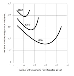
Moore’s paper stated that one could achieve a 2X complexity increase every year. In other words, the ideal density point doubled with every generation, while the cost per component halved.
Moore’s Law was therefore an economic model. Gordon Moore used less than 10 years of industry data to predict—with remarkable accuracy—the next 60 years of the electronics industry. It also became the industry’s roadmap, which defined that each logic node would have twice the density of its predecessor.
From this original definition, many people have defined “Moore’s Law” as encompassing the four critical semiconductor metrics of Power, Performance, Area, and Cost (PPAC). In this extended definition, Power was described as halving at each generation, while Performance doubled. However, this timeframe has extended from the original one-year cadence up to 18 months, and then to two years.
Yet, Power and Performance were the first two metrics to “fall off” the Moore’s Law curve. Transistor power reductions slowed nearly 20 years ago—each successive node generally reduced active and standby (leakage) current, but not at the 2X reduction per node. Transistor performance gains slowed shortly after; again, each node is generally faster, but not by 2X.
It’s in the original definition where there can be some debate as to whether Moore’s Law has slowed. If one looks solely at transistor size, then of course Moore’s Law is slowing, since the area per transistor is not shrinking by 2X each generation. Meanwhile, node naming conventions such as “180 nm” used to refer to the transistor gate length; it now has no relationship to any transistor dimension, and minimum gate lengths are quite larger than the corresponding node name.
However, if one considers “area” to be chip area or density as measured by transistors per mm2, then this metric has probably remained the “truest” to Moore’s Law. Leading manufacturers continue to achieve density improvements that aren’t far from Moore’s Law.
In logic, for example, TSMC’s 3-nm N3 process is forecast to provide a near-Moore’s Law 1.7X chip density improvement over its 5-nm N5 process—and on a two-year cadence. The entire semiconductor ecosystem has enabled this through constant innovations in materials, device architectures, and breakthrough tools such as EUV.
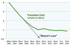
Where Moore’s Law has slowed or even reversed, however, is the cost per component. Doubling density used to cut the cost per transistor in half, which was the primary enabler of the electronics revolution. Moore’s Law meant we’d get twice the number of transistors (which were faster and less power-hungry) for the same cost.
As the chart (Fig. 2) shows, this began slowing at the 40-nm node, and virtually stopped when the industry moved to FinFETs. New nodes enable “close-to-Moore” chip-size scaling, but this is nearly completely offset by exploding wafer-fabrication costs. Various analyses show fabricated wafer costs increasing 3-5X over the 28-nm node, with 5-nm wafer costs approaching $18K each.
Therefore, it’s clear that the Moore’s Law cost reductions we used to see are slowing significantly. We can still increase functionality each generation by cramming nearly twice as many transistors on a chip, but these “super chips” will cost more, not less, than their predecessors. This will have a profound impact on the semiconductor industry:
- "Easy" electronic product cost and performance gains one used to get from Moore's Law scaling has slowed. Chip designers therefore invest more in product design and differentiation rather than slavishly chasing the latest nodes.
- Advanced nodes are only attractive to CPUs, FPGAs, and mobile processors; design costs become prohibitive for all other applications. This trend has been underway for some time, but the reduced gain from using the most advanced nodes accelerates this.
- Product lifecycles lengthen. Previously, each product generation was the best that could be achieved, only to be eclipsed by a subsequent superior generation. Today’s electronic products have a longer useful life because newer products will not offer as much relative improvement as they once did. This could lead to a significant reduction of semiconductor demand. However, it will be somewhat offset by the growing market for semiconductor products in long-life products such as automobiles and industrial equipment.
In summary, Moore’s Law both is, and is not, slowing — depending on which aspect you look at. What’s clear is the areas that are slowing will have a major impact on the industry.
What do you think the shortage has shown us?
The shortage has led many industry observers and government officials to discuss the need for increased capacity through the building of new fabs. Unlike many other technologies in the global supply chain, the combination of capital intensiveness and latency comes at the price tag of billions of dollars and years to be up and running. Thus, chip supply can’t meet drastic fluctuations in JIT (just-in-time ordering), so it does little for today’s imbalance.
This also runs the risk of causing a major hangover effect and cyclicality—a capacity boom comes online just as demand wanes, leading to a massive over-capacity problem. The capacity problem isn’t just at the leading edge; in fact, some of the biggest constraints are in the legacy 200-mm fabs.
Investing in the trailing edge is problematic because the wafer pricing model for these fabs is typically based on the capital equipment being fully depreciated. Investing in additional capacity means adding a cap-ex depreciation cost onto the wafers, putting the fabs that invest at a competitive price disadvantage to those fabs who don’t invest and therefore don’t increase prices.
This is a prime opportunity to incorporate non-capital investments to increase fab throughput with minimal CapEx. Examples are new materials such as Atomera’s Mears Silicon Technology (MST), redesigned fabrication or metrology flows that streamline wafer throughput, and other engineering techniques.
It’s about improving yields. We need technologies that will allow semiconductor fabs to extend the life of their expensive manufacturing facilities by providing a new, unexpected suite of material improvements within the existing process node.
Atomera’s MST can address the imbalance without the hefty price tag and the time needed to build new fabs. It combines innovative materials, structures, and device physics, thus enabling precise semiconductor engineering, especially when fab companies are hesitant to invest in trailing edge node technologies, with the goal to perfect the semiconductor process.
Do you think that More-than-Moore technologies will have a bigger role going forward?
Absolutely! Let’s first list some of the primary More-than-Moore (MtM) technologies:
- New packaging technologies (SiP, etc.)
- Power/HV/RF technologies
- CIS and other sensors
- New memories (MRAM, ReRAM, etc.)
Let’s consider the first two on the list. New packaging is perhaps the most significant of these because it enables chiplets and other heterogeneous wafers to be combined almost as if they were on the same die. This will have profound implications across the application and technology landscape.
Power, HV, and RF are three of the fastest-growing semiconductor markets; power and HV because of the growth of sophisticated power management (PMIC) in all applications and the growth of automotive, industrial, and infrastructure; RF because of the growing sophistication of mobile communications in 5G and soon 6G.
These markets fit the classical definition of “More than Moore” because many of the large switches and other devices require certain physical dimensions and don’t scale in the traditional sense of Moore’s Law.
One of the best ways to shrink and/or improve these devices is to use new materials. Atomera’s MST has been shown to significantly reduce the size of these large power switches by 30% or more using the same process node and equipment set.
Companies also are increasing their efforts in using silicon-carbide (SiC) and gallium-nitride (GaN) substrates to make lower-cost, lower-loss power devices. More-than-Moore technologies are the solutions to the chip supply-chain disruptions, now and in the future, and can protect the industry from future shortages like this.
Can you please elaborate on what “MST” is and how it can benefit the industry?
MST (Mears Silicon Technology) is a new material that provides benefits to all nodes across the semiconductor industry, from the very latest gate-all-around and nanosheets, to legacy planar fabs.
The MST film provides a number of benefits to semiconductor devices:
- It strongly blocks dopant diffusion, enabling the design of precise and well-controlled semiconductor junctions.
- It increases transistor drive current, enabling smaller size and/or lower-power devices.
- It reduces Vt mismatch, which is critical for sense amps and analog circuits.
- It reduces gate-oxide leakage.
- It improves TDDB and NBTI reliability.
MST is a material that was designed “bottoms up” using ab-initio quantum mechanical design. It acts as a thin film that can be inserted onto the top of a silicon wafer to enhance semiconductors. The most common form of MST still uses silicon and oxygen, probably the best-known and most characterized materials in the semiconductor industry. However, the layered arrangement of these atoms yields a host of desirable properties for engineering silicon devices, from tighter interface control and more precise placement of dopants to improved electron and hole mobilities.
Depending on the target process and desired improvement, MST has been demonstrated to:
- Reduce die size by 15-20% without the need to build new fab.
- Provide a 30% increase in performance.
- Deliver a lower-cost, quicker ROI.
- Improve transistor characteristics and thus lower power consumption.
- Achieve ~1 node transistor improvement without requiring major changes to process or CapEx.
With more than 20 years of advanced development, Atomera’s MST gets the industry closer to achieving the perfect semiconductor, and addresses many of the challenges within the industry.
What are the challenges with manufacturing semiconductors, and how is MST different from other approaches that are being attempted?
New materials require a long time-to-market development cycle, from 15 to as long as 18 years, because there’s no margin for negatively impacting the manufacturing process in the semiconductor industry. To address that challenge, MST can be fabricated using existing epitaxial tools that are already commonplace in the fab. One attractive property of MST is that it uses well-understood elements that don’t pose any contamination issues.
MST is embedded into the silicon wafer early in the manufacturing process and then forms a barrier that inhibits dopant diffusion, enabling a much thinner layer of epi-grown material at a lower cost and higher purity for device fabrication. Since this is a layer added into the current manufacturing process, it means that there’s no need to build a new fab to support the process.
The uniqueness of MST lies within the value it brings to the existing semiconductor process rather than starting the process over. MST has already gone through the typical R&D period of a new material and is set to find widespread application.
About the Author

William G. Wong
Senior Content Director - Electronic Design and Microwaves & RF
I am Editor of Electronic Design focusing on embedded, software, and systems. As Senior Content Director, I also manage Microwaves & RF and I work with a great team of editors to provide engineers, programmers, developers and technical managers with interesting and useful articles and videos on a regular basis. Check out our free newsletters to see the latest content.
You can send press releases for new products for possible coverage on the website. I am also interested in receiving contributed articles for publishing on our website. Use our template and send to me along with a signed release form.
Check out my blog, AltEmbedded on Electronic Design, as well as his latest articles on this site that are listed below.
You can visit my social media via these links:
- AltEmbedded on Electronic Design
- Bill Wong on Facebook
- @AltEmbedded on Twitter
- Bill Wong on LinkedIn
I earned a Bachelor of Electrical Engineering at the Georgia Institute of Technology and a Masters in Computer Science from Rutgers University. I still do a bit of programming using everything from C and C++ to Rust and Ada/SPARK. I do a bit of PHP programming for Drupal websites. I have posted a few Drupal modules.
I still get a hand on software and electronic hardware. Some of this can be found on our Kit Close-Up video series. You can also see me on many of our TechXchange Talk videos. I am interested in a range of projects from robotics to artificial intelligence.
Comment About the Article
To join the conversation, and become an exclusive member of Electronic Design, create an account today!

Leaders relevant to this article: