Delivering 2D Materials Ready for a “More than Moore” World
What you’ll learn:
- The need to industrialize 2D materials to extend Moore’s Law.
- The challenge of manufacturing 2D materials at scale.
- The solution to the problem of how to industrialize 2D materials.
The International Technology Roadmap for Semiconductors (ITRS) has clearly identified transistors based on 2D materials as one of the key technologies that will offer a long-term solution for extending Moore’s Law. Indeed, the properties and predictable electrical characteristics of 2D materials offer strong potential to continue to extend the remarkable innovation and performance gains we’ve witnessed in the semiconductor industry in the last 50 years.
However, the ITRS isn’t a guarantee that these materials will deliver on this potential. There’s no doubt that the world’s leading semiconductor manufacturers like Intel and TSMC are very keen to understand the manufacturing implications of 2D materials. But, for all of the academic papers in the past 10 years, even the most researched material—graphene—is nowhere near ready for deployment in full, high-volume manufacturing (HVM) production facilities.
The challenge of HVM for 2D materials is significant. But that challenge holds the key to ensuring that 2D materials deliver on the potential, rather than squandering it in a catch-22 of hype.
The Need to Industrialize 2D Materials
Adopting new materials in the semiconductor industry is a hugely disruptive process. However, there are few technological guarantees when it comes to extending Moore’s Law and securing the continued growth of a $600 billion market. As such, the concept that 2D material manufacturing can evolve to play a critical part of the global semiconductor market is definitely not idle speculation.
Despite this, the reality of the technology today is that 2D materials have only ever been grown in small quantities in laboratories to support academic research. Rather than rushing to publish yet another research paper on the amazing potential of graphene, there’s increasing focus on developing the tools, processes, and equipment necessary to manufacture high-quality graphene, or other materials, at an industrial scale.
Integrating 2D materials into mainstream manufacturing at industrial scale involves some tough engineering—covering material growth, material transfer, and production line integration. In many ways this is the “unglamorous” work, but it’s essential if 2D materials are going to achieve their potential.
The Scale of the Challenge
The key to the future of 2D materials is designing tools and processes that produce defect-free materials applicable to existing industry-standard 200- and 300-mm wafers. However, achieving that is easier said than done.
Every step of the process requires specially engineered and extensively customized production tools. It’s worth bearing in mind that these are highly specialized materials—one atom thick—which need to be structurally perfect and free of impurities to perform.
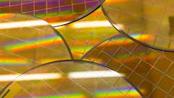
Starting with material growth, chemical vapor deposition (CVD) is the most widely used process to produce graphene and other 2D materials, such as hexagonal boron nitride.
Producing graphene involves exposing a heated substrate to carbon-containing gases in a vacuum. As the gas settles on the hot substrate surface, carbon grows into graphene’s distinctive honeycomb pattern. This process requires stringent control of temperature and other parameters to ensure that high-quality material can be grown to the required wafer size.
The growth process is then followed by the dry transfer process, which separates the material from the growth substrate and moves it to the production wafer. This task is akin to attempting to pick up a football-field-sized sheet of plastic wrap and depositing it on an adjacent field—all without breaking or contaminating any part of the material surface.
And, of course, the need for specially engineered equipment is heightened by the fact these processes also must be implementable within the highly automated production processes found in fabs.
The Development Path
Given the technical challenges involved, there’s not going to be a single “leap” forward where we jump from today’s small-scale material growth to full HVM production. However, with the IEEE Roadmap for Devices and Systems (IRDS) as a guide, we can see that some key technology “stepping-stones” will help the industry develop and prove the tools and processes required to facilitate the transition to 2D materials.
The first of these stepping-stones is in commercial back-end-of-line (BEOL) applications. These are the final stages of certain production processes where special functions like sensing or photonic switching are added to the semiconductor wafer. They represent strong opportunities for graphene producers to hone their production tools.
Such devices tend to be produced in foundries operating at lower volumes and have already transitioned to added BEOL technologies such as microelectromechanical systems (MEMS). As a result, there’s more flexibility to accommodate planarized 2D layers into the production process in collaboration with graphene manufacturers.
These BEOL applications will be crucial to proving that graphene can be credibly grown and deployed in a commercial production environment.
Delivering on the “More than Moore” Potential of 2D Materials
These initial applications are critical steps in developing the automated systems and process control required to ensure highly consistent material results.
At ANL, we’re committed to furthering this commercial acceleration. Application development kits will enable more customers to shorten the path to integrating 2D materials in a host of other applications. And industry collaborations with new ecosystem partners will help supply engineering volumes of graphene to companies developing prototype devices.
Ultimately, this vital groundwork in the next few years will see 2D materials move out of the lab and gain momentum as a true “more than Moore” commercial HVM proposition. The development of fully integrated end-to-end production tools will ensure that when semiconductor manufacturers are ready to move into full production, the industrial growth, transfer, and integration propositions will all scale with them.
About the Author
Paul Hedges
CEO, Applied Nanolayers
Comment About the Article
To join the conversation, and become an exclusive member of Electronic Design, create an account today!

Leaders relevant to this article: