Material Evidence: How Laminate Properties Impact the PCB Design Process

This article is part of the TechXchange: PCB Tools and Technology
Members can download this article in PDF format.
What you’ll learn:
- Why today’s high-speed, high-frequency designs have very little “wiggle room” within them relative to laminate properties.
- Why the end-product’s application and performance determine the most critical laminate-related properties.
- Why “beyond-the-datasheet” laminate information is imperative for an optimized design.
Numerous strides have been made in the tools and technologies used to design, manufacture, assemble, and test printed circuit boards (PCBs). At this point, it might be readily assumed that due to the long history of PCB fabrication, the PCB design process doesn’t have any major “gotchas.” But that’s not the case, and they often come in the form of the physical properties and performance characteristics of the laminates used to make PCBs.
In particular, as we go up the performance curve with today’s high-speed, high-frequency applications, there’s a greater need to focus on how these factors impact product design, manufacturability, operability and reliability.
At the highest level, the challenges with laminates are twofold:
- Accounting for all properties and characteristics that are beyond the “basics.”
- Assessing the laminate-related issues for your product and addressing them early in the design process.
This article will address these challenges by providing the upper-level guidelines for the laminate evaluation and selection process. It also highlights which properties and characteristics can impact your design based on the final end-application of your product.
A Brief History of Laminate Choices
For a very long time, PCB material choices were limited to some combination of epoxy-glass and polyimide that came to be classified as FR-4 laminates and other ANSI grades. These laminates were the workhorses of the industry, and they’re still in wide use today. The performance characteristics of importance in these laminates was thermal properties and processability, and that’s since shifted to low permittivity (Dk) and loss tangent (Df).
However, while FR-4 laminates were widely used even in the “dark ages” of PCB designs, some “fringe” applications—such as those found in mil-aero or defense products—specified a different laminate with little known about their long-term manufacturability, operability, or long-term reliability.
For example, when I was an engineer at Martin Marietta several years back (more than I care to admit), the PCB material of choice for the Low Altitude Navigation and Targeting Infrared for Night (LANTIRN) program was Kevlar. LANTIRN was a combination of navigation and targeting pods that were mounted underneath the wings of fighter aircraft (e.g., F-15 and F-16). Thus, the boards in them had to operate reliably in a ruggedized, harsh environment at high temperatures.
While Kevlar fit those environmental conditions, what we didn’t know was that Kevlar-based boards were subject to “measling, crazing, and haloing” due to the fab process. The fabrication specification levied on our program, MIL-P-55110, prohibited these “defects.” In turn, all efforts came to a screeching stop while we went through an extended QA process to verify that these cosmetic flaws would not affect the operation and reliability of the two-pod system.
These days, it’s difficult to imagine any product development effort could withstand the kind of stoppage noted above. However, our industry has morphed to the point that PCB laminates are pushed to the edge to satisfy today’s high-speed and high-reliability performance requirements. It’s actually more accurate to state that today’s PCBs and the laminates used within them have very little flexibility or “give” in terms of their operability and reliability.
Presently, single points of failure in any aspect of the design, including the PCB and its structural components, can spell the end of a particular design, end-product, or program. And, when we discuss the importance of PCB laminates, it’s necessary to consider the broader business aspects associated with their use: the need for redesign, expensive non-recurring engineering costs, multiple respins of boards, missed product windows, and reduced profit margins.
What’s Important in Today’s High-End and Mainstream Designs?
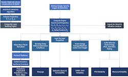
Beyond the fundamental attributes of Dk and Df noted above, other equally important laminate-related factors contribute to the function of a device and its long-term survivability. These include mechanical and thermal properties such as stiffness, expansion coefficients, properties of copper, and copper roughness. These properties not only the address the processability of the materials, but also the field reliability of the product. The figure shows the workflow that goes into the laminate evaluation and selection process.
In many cases, it’s the end-application and performance of the products that dictate which laminate-related properties are the most crucial. For high-end boards found in routers and servers, the speed of processing the data is the key aspect. For handheld devices, in addition to their computing capabilities, other factors of concern include their ability to withstand multiple drops, tolerate vibrations, or withstand high heat such as that found in a car’s interior. It’s important to keep in mind that all of these performance requirements directly relate to the intrinsic characteristics and properties of the laminates from which they’re constructed.
While all of the foregoing factors play a role during the material evaluation process, the challenge is that not all laminate suppliers do the investigation required to determine whether their laminates will support those factors.
Types of Tests Being Done
The types of tests that most laminate suppliers will perform are CAF testing and thermal testing. CAF (conductive anodic filament formation) is a process wherein the conductive chemistries are transported across a non-metallic substrate under the influence of an applied electric field. It’s influenced by electric field strength, temperature (including soldering temperatures), humidity, laminate material, and the presence of manufacturing defects. As noted later in this article, CAF is often responsible for field failures in humid environments.
At the behest of the automotive manufacturers, some laminate suppliers also will conduct thermal cycle testing. In these situations, an OEM automotive supplier will provide the information to the laminate provider and state “subject the laminate to alternating thermal cycling conditions simulating an Arizona summer to a Canadian winter.” It’s important to note that only a few laminate suppliers will do this kind of cycling.
The Influential Elements Within Laminates
Years back, when “high-speed” end-applications were operating at a few gigahertz, lots of latitude was given in terms of the impact laminate properties and characteristics had on final products. In contrast, now, as we push to 112 Gb/s in current designs, there’s not much leeway at all, especially for the aforementioned Dk and Df characteristics.
In addition, the loss budgets for these high-speed devices are extremely low and, in most cases, they’re beyond the capabilities of both the laminate and the conductive, which is copper. As a result, the choice of materials and the copper widths become very critical.
With early mobile devices, many instances of bad designs made it to market. And, a lot of the “failures,” such as glass shattering, were left to the next rev of the design to ameliorate the problem.
In mission-critical designs, there’s no room for the error that can lead to the failure of an entire system, and it’s not possible to wait for the next product iteration to address the problem. Thus, these designs must be robust in terms of their ability to perform multiple functions, reliably, over a long period of time. For such designs, it’s the interplay of the thermal/mechanical properties like expansion, Tg, modulus, shear properties, and fracture toughness that has to be taken into account.
The foregoing describes the key elements in getting a board manufactured. However, the PCB manufacturing process itself also is very demanding and grueling. In almost all instances, it takes materials well above their elastic regions.
The processes of lamination, drilling, and reflow place stresses and strains on the laminate that put them at their breaking point. And, ultimately, very small deviations can lead to the failure of a design. We don’t see 6 sigma kinds of numbers in our industry and yields tend to be between 70% to 90%. If the laminate in a board can’t survive these processes, you’re right at the very end of what is achievable, and designs can fall off.
Why You Can’t Rely on Just One Data Point for Your Design
Just as we examine the tradeoffs in a PCB design between manufacturing, assembly, reliability, test, and cost, there’s a need to examine the properties within laminates to see how well they play with each other. That’s what’s been at the core in the development of our Gauss Stack product. It enables you to look at the impact of these properties for a given material, in a given design, and determine whether they will work well together or if everything needs to go in another direction.
With certain high-speed designs, which are HDI types, multiple, sequential laminations are required. So, in addition to the low Dk and Df, low levels of CTE and high adhesion are needed as well, not to speak of thermal robustness. However, when you add something in the laminate system to have low CTE, it will adversely affect the dielectric properties and adhesion.
The final laminate choice must strike the optimal balance between product performance, the ability to survive field conditions, and the inclusion of low CTE. It’s a delicate balance to arrive at a good design that fulfills all operation requirements and performs optimally in field operations.
As noted earlier, the challenge is that laminates are composites comprised of polymers and reinforcements such as glass and fillers. That’s why having just one data point from a datasheet isn’t sufficient for most designs.
When properties are limited to Dk and Df, the data on mechanical properties (modulus, expansion, and CTEs) aren’t available. Whether you’re building high-layer-count boards or those that are four- or six-layer, you can’t just rely on a single data point for your design.
To further complicate matters, for a number of years, and somewhat still today, there are instances where the data in a datasheet is wrong. Because product developers may not have experience with all of the properties and characteristics of a given laminate, they can’t determine if the information provided is questionable. Fortunately, we’ve seen this problem be fairly well eradicated because laminate suppliers have been called out on supplying incomplete or erroneous data.
Going in the opposite direction, some laminate suppliers will overstate their Dk and Df numbers. Then, when product developers simulate their numbers, they will achieve better results in practice. This actually adversely affects the laminate supplier, but as long as they are getting sales, they tend not to worry about the errors in their data.
How Product Development Efforts Factor into the Equation
A key challenge in understanding the interaction between laminate properties comes from how interactions are handled during the product development process.
For years, our industry has been characterized by people working in silos even within OEM groups. Designs are handed over from the electrical to the mechanical designers. And, when these groups only rely on the information on material datasheets, it often diminishes the needed interplay and multidisciplinary approach to product design.
Taking this one step further, those in charge of designing the product don’t understand what the laminate properties and characteristics can do to their product because they don’t see this impact at their level.
This has been the source of practices such as rework and respin, which are embedded in the design process and typically considered to be part of the price of “doing business.” But what frequently happens is that product launches can get delayed, stymied, or shelved because the laminate information wasn’t correctly considered during the design process.
Another frequent occurrence is that software and modeling tools tend to over predict the performance for a specific laminate. This is especially true in the case of loss. Then, when failures occur, the product developers will ask the laminate suppliers why their laminate isn’t working, while the laminate supplier will ask why they weren’t involved in the evaluation process during the earliest phases of the design effort.
Part of the problem is that much of the product development activity is driven by purchasing departments. This is best described as the “cost vs. price” business model. Laminate selected at the lowest cost can result in the highest price when it’s found that the end product is flawed or doesn’t work at all.
One of the best ways to ensure that the product you’re designing is manufacturable, operable, and reliable across the entire product lifecycle is to involve everyone in the design process. The laminate supplier, the product developer, and the manufacturer are equally important. In some instances, it’s necessary to involve the assembly and test groups as well.
Verification vs. Validation
Though several good verification software products are available to the industry, the only way to know for sure that your product will work as designed and manufactured is to do real-world validation.
Within our Gauss software, we enable our customers to screen several materials and their expanded properties and characteristics. Then they move to the next stage, which is to do validation on two or three prototypes. At the end of the day, real-world validation is the only way to ensure that your design will work as designed and manufactured.
The foregoing practice isn’t without its challenges. With a lot of secrecy surrounding new builds, product developers don’t want to send their design to a fabricator that may significantly compromise that secrecy (as has happened in some offshore facilities). Also, real-world validation is expensive. Fabricators can ask for and get hundreds of thousands of dollars to validate a design.
Doing the validation computationally is great but may not always be available as a solution. On top of that, the level of technology involved is another problem. For instance, if you want to build a board with microvias or stacked microvias, there are only a few manufacturing facilities that can do that kind of manufacturing.
In addition, such complex high-end designs only account for 6% to 7% of the boards being built for the entire PCB market. As a result, people will do validation builds like volume runs and spend between hundreds of thousands and one million dollars just to get their product validated.
Unfortunately, if you haven’t taken the steps necessary to ensure that your design is manufacturable, you end up going back to square one. Fine-tuning the verification process wherein you narrow the options down to two or three prototypes is the most effective way to arrive at a real-world, validated design.
Other Challenges
Taking all of the foregoing into account may not be enough when it comes to material properties and characteristics. One of the biggest impacts on a type of laminate is aging of the material. When the lead-free conversion happened, a great deal of material was brought onto the market almost immediately. Only later was it discerned that the material didn’t work too well with humidity. CAF is the classic example of what can happen over time and lead to field failures.
Bottom line, something that absorbs moisture will degrade over time. You can do signal-integrity work with pristine dry material that works fine in a dry environment. Then when the product is running in hot, humid conditions in some other environment, the material will degrade over time and the product won’t perform as specified or perform at all.
Again, taking into account all of a design’s performance characteristics in terms of its inherent operation, as well as the environment into which it will be deployed, goes a long way to ensuring that the product will perform correctly.
Why the Stackup Design is So Important
One of the key efforts involved in any successful PCB design is creating a really good stackup. Unfortunately, it’s necessity and exactitude are often not given near enough consideration. Seemingly benign changes to the prepreg layer or the stackup, or replacing one laminate with another that has a higher or lower resin content, can lead to warpage, make the board unmanufacturable, or lead to CAF problems.
Not long ago, we witnessed a design where the glass type in the laminate was changed, resulting in massive voids. The outcome was that the entire product was shelved after two years of development effort. It was a disastrous result and could have been prevented if someone had addressed it at the onset of the design process.
Unknowingly, product developers may think that adding or removing a layer or replacing 1 oz. copper with 2 oz. copper won’t make any difference—and then they’re left to wonder why their boards are delaminating. Paying proper attention to the stackup process, understanding how specific materials properties will affect design, and taking as many downstream processes into account early on in the design effort goes a long way to achieving a properly designed and built product that’s also profitable.
What Factors Should You Consider in Your Design?
While the impact of laminate selection is based on the end-application of your product, here are some of the main laminate-related issues that you will want to avoid in your final product. Technology now exists to address them proactively during the creation of the stack-up design.
- Glass stop and resin starvation
- Filler damming
- Plated-through-hole reliability
- Microvia reliability
- Solder-joint reliability
- Dielectric stress
- PCB warpage
Summary
We’ve come a long way when it comes PCB design, manufacturability, and operability. For those of us who have been in the industry a long time, each new product development challenge creates lots of head scratching as we determine if the end product can be developed using traditional design approaches and laminate materials. Nonetheless, we do so.
Then the next product innovation comes along, and we start to wonder again how we will overcome the technology hurdles required to build it. That’s the challenge and it’s what makes all of us get up in the morning.
About the Author
Kella Knack
Director of Strategic Marketing, Avishtech
Kella Knack currently serves as Director of Strategic Marketing for Avishtech, a leading provider of EDA software design tools—Gauss Stack and Gauss 2D. She assists in the company’s marketing communications, PR, and outbound messaging efforts.
Previously, she served as Vice President of Marketing for Speeding Edge, an engineering consulting and training company focusing on the design of high-speed PCB and system design. Before that, she was the Founder and President of KJ Communications, Inc., a marketing consulting and public-relations company based in Silicon Valley. She served as a strategic adviser for several highly successful marketing campaigns for clients that ranged from startups to multimillion dollar companies in the EDA, networking, SOC IP, semiconductor, embedded-system design, and database-management market sectors.
Comment About the Article
To join the conversation, and become an exclusive member of Electronic Design, create an account today!

Leaders relevant to this article: