Designing with Ultra-Thin, Flexible Printed Circuit Boards
Download this article in PDF format.
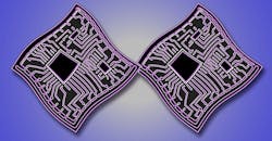
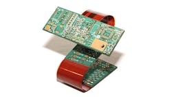
Flexible printed circuit boards (PCBs) aren’t much different than rigid boards during the design phase, except that the designer must account for the mechanical complexity associated with flex circuits (Fig. 1). For instance, a flexible PCB can tear if flexed beyond its capability during installation.
Therefore, it’s very important to create a mechanical model of the PCB and test it for a proper fit, before taking up the electrical design. This would also involve testing the ergonomics of the installation, any misalignments, and servicing. In addition, it necessitates that designers understand the different types of flex circuits available and the way they work.
Types of Flexible PCBs
Depending on the application, several types of flexible PCBs are available, chief among them being the flex, rigid-flex, and the high-density-interconnect (HDI) flex.
Flexible PCBs
These are flexible versions of the commonly available rigid PCBs, with unique capabilities such as flexibility and vibration resistance. The extra features come along with the usual reliability, repeatability, and high density already offered by rigid PCBs. The major advantage over rigid PCBs is flex circuits have the ability to assume three-dimensional configurations. One of the most common applications of flexible PCBs is as a replacement for wire harnesses.
Rigid-Flex PCBs
These PCBs are a blend of the rigid and flex, offering the best of both constructions, while adding some unique capabilities that neither possesses alone. For instance, a typical rigid-flex configuration would be a series of rigid PCBs linked by integrated flex circuits. By integrating rigid areas added to the flexible parts, designers can greatly increase the design capability of their circuits.
While the rigid areas are excellent as hard mounting points for chassis, connectors, and components, the flex areas offer dynamic flexing, vibration-resistance zones, and flex-to-fit. Such blending offers designers multiple options for arriving at creative solutions for the most demanding applications.
HDI Flexible PCBs
High-density-interconnect PCBs are useful when the options offered by typical flexible circuits aren’t adequate. HDI flex circuits offer better design, layout, and construction options by incorporating fine features such as micro-vias. Increased functionality, smaller form factor, and highly dense flex circuitry are among their features.
Although it uses thinner materials, HDI technology provides better reliability, improved electrical performance, and access to advanced IC package use.
Advantages of Flex Circuits
As a replacement for a ribbon cable, or discrete wiring, flex circuits supply customized repeatable routing paths throughout the assembly. Flex circuits can reduce service calls due to their greater dependability.
Flex boards cover their conductors with polyimide, a dielectric layer that protects the circuit better than the simple solder mask. Manufacturers use other base and cover materials to handle a broader range of ambient conditions and harsh environments.
Although flex boards can be very thin, they’re able to weather long duty cycles of flexing. Using suitable design material, they can be made robust enough to withstand millions of flexing cycles, while carrying power and signal without interruptions.
The low mass and high ductility of flex circuits is a huge advantage when facing high acceleration and/or vibration. The stress and impact on itself and solder joints on the flex PCB are far lower than that faced by the solder joints and components on a rigid PCB under the same working conditions.
Uses of Flex Circuits
Designers shape flex circuits to fit where it’s impossible to use any other type of PCB. One can think of flex circuits as being a hybrid combination of the ordinary PCB and round wires, while exhibiting their individual benefits. With flex circuits, one can retain the precision, density, and repeatability of regular PCBs, and still achieve unlimited freedom for packaging geometry.
Flex circuits are commonly used to replace the wiring harness. This allows a single flex circuit to supplant several connectors, cables, and hardboards in one operation. The assembly proceeds much faster, because it eliminates the need to color-code wires and wrap them in bundles. Volume production levels go up, while installation costs come down, and there are lower chances of rejects during assembly and in-service failures.
Replacing wire harnesses with flex circuits increases the repeatability of wire routing. It eliminates errors during wire routing, thus reducing rejections, rework, and test times. The connections are more robust, because flat foil conductors can dissipate heat better and carry more current than round wires of the same cross-sectional area. As the designer decides on a more uniform conductor pattern in a flex circuit, the impedance, crosstalk, and noise will be better controlled.
Furthermore, use of flex circuitry can reduce the space and/or weight of conventional wiring by up to 75%. Compared to the use of wire harnesses, the recurring costs of flex circuits are lower. As flex circuits are more resistant to vibration and shock, costs for repair and replacement are far lower compared to those incurred for hard boards. Moreover, by placing bonded stiffeners at required areas, surface-mount components can be easily mounted on flex boards.
Advantages of Rigid-Flex Circuits
Flexible circuits provide advantages over rigid PCBs, but they also come with more design considerations.
When reviewing the entire installation for the total cost of ownership, use of a rigid-flex circuit is advantageous in the fact that it replaces the maximum number of components. Not only can surface-mount components be mounted on both sides of the board, rigid-flex circuits make it possible to integrate the best capabilities of the resilient flex areas with the resistant rigid areas, thereby offering the highest capability and maximum vibration resistance. Since it offers the smoothest transition between rigid and flex areas while preserving the benefits of each, this combination is the best option when mounting a component with a high mass.
HDI Stackup
One of the most important aspects in the initial design of a multilayer PCB is defining its appropriate stackup. This is essential for large, dense PCBs with multiple pin-count BGAs, especially when standard laminate stackups are inadequate in terms of cost and performance goals. HDI stackups are a viable alternative to large number of layers providing lower cost with higher performance if properly designed.
For boards with high pin-count BGAs, there can be three types of stackups—standard lamination with through-vias, sequential lamination with blind and buried vias, and buildups with micro-vias. Of these, HDI boards primarily use a buildup with micro-vias, because it offers several advantages:
- The vias and traces have smaller feature sizes, leading to higher routing density and fewer layers.
- Micro-via patterns can be more effectively used, which opens up more channels for routing and leads to potentially fewer layers
- This is the only practical way for designing with multiple large BGAs with pitch less than 0.8 mm.
- Offers the lowest cost for high-density boards.
- Appropriate stackup definition leads to improved signal and power integrity.
- Appropriate materials for processes that must meet RoHS standards.
- Newer materials are available for higher performance at lower costs, but these new materials may not be suitable for other types of laminations.
Eminent PCB manufacturers have defined HDI PCB stackups with 16 layers, where the overall board thickness is only 66 ± 7 Mils. This requires sequential build-up (SUB) and has laser-drilled micro-vias.
The Impact of Cost
Although flexible circuits are more expensive than rigid PCBs, the costs generally rise with the layer count. Therefore, options may have to be considered to minimize the cost. For instance, two double-layer circuits could turn out to be less expensive compared to using one four-layer circuit.
Other factors may lower the overall cost in favor of flex circuits. For instance, the ability to fold a flexible circuit could save space and layers. Depending on the situation, time invested in project assessment has the potential to result in significant overall savings.
Akber Roy is the CEO of RUSH PCB Inc. He has 20 years of experience of electronic contract manufacturing. RUSH PCB’s website provides detailed printed-circuit-board development resources.

About the Author
Akber Roy
CEO, RUSH PCB Inc.
Akber Roy is the CEO of RUSH PCB Inc. Akber Roy has 20 years of experience of electronic contract manufacturing. RUSH PCB’s website provides detailed printed-circuit-board development resources.
Comment About the Article
To join the conversation, and become an exclusive member of Electronic Design, create an account today!

Leaders relevant to this article: