An Examination of LPWAN Technology in IoT
The explosive growth of the Internet of Things (IoT) is leading virtually every industry to incorporate connected technologies to ensure it’s ready to move toward an automated society. Our daily lives continue to evolve alongside technology as homes, cars, wearable devices, healthcare devices, cities, utilities… everything is becoming connected and interactive, and more data about us is transmitted across networks and saved in the cloud.
Network requirements of the IoT demand communication technologies that offer long-range connectivity, low power consumption, and affordable expansion. Low-power wide-area network for IoT, or LPWAN, technology was created to meet these needs.
LPWAN for IoT
According to the Global Standards Initiative on the IoT, a device labeled as IoT must meet seven criteria related to sensors, internet connectivity, processors, energy efficiency, cost-effectiveness, quality and reliability, and security. To be attractive for use in commercial applications, IoT devices need to factor in low power consumption, long distance communication, and affordability.
Comparison of the features of key wireless standards.
Applications like smart meters require a long battery life—up to 10 years without charging—as well as long distance connectivity, but the widely used Bluetooth, Zigbee, and other short-range communication technologies cannot meet these requirements. Currently available cellular mobile networks, e.g. 2G, 3G, and 4G, meet the long-distance communication requirements of the IoT applications, but the high power consumption required to operate on these networks isn’t compatible with use in IoT devices. To meet the requirements of the rapidly growing IoT market, LPWAN technologies have been introduced.
Comparison of the key technical features of LPWAN standards for IoT applications.
Currently, four main LPWAN technologies are available in the market for IoT devices: LoRa, Sigfox, Narrowband IoT (NB-IoT), and Long-Term Evolution (LTE) Category M1 (LTE-M).
LoRa
LoRa was developed by French wireless long-range IP provider Cycleo SAS, which was acquired by Semtech in 2012. LoRa is a physical-layer technology that modulates the signals in the sub-GHz ISM band using chirp spread-spectrum (CSS) modulation technology. CSS was developed in the 1940s and was traditionally used for military applications because of its long-distance communications capabilities. LoRa’s data rate is between 300 bits/s and 50 kbits/s. It uses bandwidth of 125 kHz and 250 kHz.
According to the LoRa Alliance, led by Semtech, there are currently 83 network operators operating in 49 countries.
LoRa Transceiver: Semtech SX1272
TechInsights has analyzed the Semtech SX1272 LoRa long range transceiver; the 28-pin QFN package is 6.0 mm (L) × 6.0 mm (W) × 0.93 mm (T). The Semtech SX1272 contains a single die. Figure 1 shows the top metal die photo and die markings. The die size (die seal edge) is 4.04 mm × 2.50 mm (10.10 mm2) and shows die markings “TL378V2.”
1. Top metal die photo and die markings found on the Semtech SX1272.
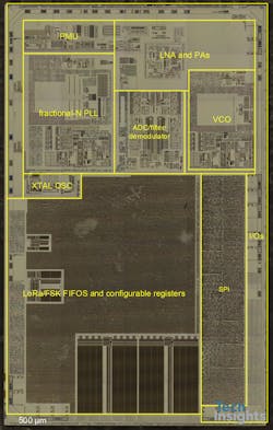
TechInsights has annotated the key functional blocks of the SX1272 die (Fig. 2).
2. Functional blocks of the Semtech SX1272 at the diffusion layer.
Sigfox
Sigfox technology was developed by the French company Sigfox. Sigfox is an ultra-narrowband technology that uses binary phase-shift keying (BPSK) modulation and a sub-GHz ISM band. Sigfox’s use of ultra-narrowband frequency results in very low power consumption.
Sigfox licenses its technology to other companies; we have seen it in chips from STMicroelectronics, ON Semiconductor, and Microchip; Sigfox claims that it has built networks in more than 30 countries.
Sigfox transceiver: ON Semiconductor AX-SFJK-API
TechInsights has analyzed the ON Semiconductor AX-SFJK-API Sigfox transceiver IC; the 40-pin QFN package is 7.0 mm (L) × 5.0 mm (W) × 0.90 mm (T).
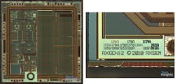
The ON Semiconductor AX-SFJK-API is a multi-chip package (MCP) that has integrated the transceiver die and CPU die in one package (since the CPU die includes only logic and memory blocks, we will focus on the transceiver for the purposes of this article). Figure 3 shows the top metal die photo and die markings of the transceiver die. The die size (die seal edge) is 2.27 mm × 2.33 mm (5.29 mm2) and die markings “AXGEN1-2” are shown.
3. Top metal die photo and die markings found on the ON Semiconductor AX-SFJK-API.
TechInsights has annotated the key functional blocks of the AXGEN1-2 die (Fig. 4).
4. Functional blocks of the ON Semiconductor AX-SFJK-API at the polysilicon layer.
NB-IoT/LTE-M
Sigfox and LoRa were the major competitors for years in the LPWAN market, before the introduction of NB-IoT and LTE-M.
NB-IoT and LTE-M are both 3rd Generation Partnership Project (3GPP) radio technology standards introduced in 3GPP's Release 13 that addresses the LPWAN requirements for IoT applications.
NB-IoT can coexist with GSM and LTE under licensed frequency bands. NB-IoT has improved indoor coverage, the support of a massive number of low throughput devices, low delay sensitivity, low cost, and low power consumption. It has a bandwidth of 200 kHz and can be deployed in 3 different modes: In-band, Guard-band and Stand-Alone. It is mainly used in low data rate applications at the 200 kbps level, such as smart meters, smart parking, smart buildings, etc.
LTE-M has similar low power and long-range measurements to those of NB-IoT, but there are a few differences between them. LTE-M has wider bandwidth, 1.4 MHz compared to 200 kHz of NB-IoT; LTE-M has a higher data rate than NB-IoT. LTE-M supports mobility and voice communications where NB-IoT does not. LTE-M is ideal for applications that require a higher data rate; for example, patient monitoring, home security, tracking, etc.
According to GSMA, there were 52 mobile IoT commercial launches in the world as of June 2018. 100+ mobile IoT modules are commercially available, as well as 20+ mobile IoT developer kits.
NB-IoT SoC: HiSilicon Hi2110 (Boudica 120)
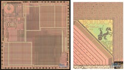
TechInsights has analyzed the HiSilicon Hi2110 (Boudica 120) NB-IoT SoC; the package is 5.3 mm (L) × 5.3 mm (W) × 1.0 mm (T), and includes 81 solder balls. The HiSilicon Hi2110 is a single NB-IoT SoC. Figure 5 shows the top metal die photo and die markings. The die size (die seal edge) is 3.83 mm x 3.83 mm (14.67 mm2) and shows the mark “Boudica.”
5. Top metal die photo and die markings found on the HiSilicon Hi2110.
TechInsights has annotated the key functional blocks of the Boudica die (Fig. 6). The HiSilicon Hi2110 NB-IoT SoC has an integrated modem, RF transceiver, PMIC and memory in one single die.
6. Functional blocks of the HiSilicon Hi2110 at the polysilicon layer.
NB-IoT / LTE-M Multi-chip package: Sequans Monarch SQN3330
TechInsights has also analyzed the Sequans Monarch SQN3330 that supports both LTE-M and NB-IoT; the package is 8.5 mm (L) × 6.5 mm (W) × 0.55 mm (T), including 300 solder balls. The Sequans Monarch SQN3330 is a MCP that has integrated the transceiver, modem, and memory dies into a single package.
Figure 7 shows the top metal die photo and die markings of the transceiver die. The die size (die seal edge) is 3.67 mm × 4.64 mm (17.03 mm2) and shows die mark “REDBELLY.”
7. Top metal die photo and die markings found on the Sequans Monarch SQN3330.
TechInsights has annotated the key functional blocks of the REDBELLY die (Fig. 8). It’s believed that the lower left corner of the die contains the transmit portion of the data path, while the upper left corner of the die is the receive portion of the data path. The clocking circuitry appears to be similar for both the transmit and receive circuits.
8. Functional blocks of the Sequans Monarch SQN3330 found at the polysilicon layer.
The explosion of the IoT market has resulted in a new type of network technology—LPWAN—that supports the long-range communications, low power usage, and affordability required by IoT standards guidance and industry use.
We have examined the four main LPWAN technologies from the reverse-engineering angle by means of semiconductor die analysis. Each technology has its advantages and will continue to have its place in the IoT market. We believe that the LPWAN market will grow very quickly in the near future, and we look forward to seeing its impact on IoT technology.
References:
Kais Mekki1, Eddy Bajic1, Frederic Chaxel1, Fernand Meyer, "Overview of Cellular LPWAN Technologies for IoT Deployment: Sigfox, LoRaWAN, and NB-IoT", March 2018.
Rashmi Sharan Sinha, Yiqiao Wei, Seung-Hoon Hwang, "A survey on LPWA technology: LoRa and NB-IoT", March 2017.
TechInsights "Semtech SX1272IMLTRT LoRa Long Range Transceiver Basic Functional Analysis", May 2018.
TechInsights "HiSilicon Hi2110 Narrowband IoT Modem Digital Functional Analysis", September 2017.
About the Author
Jefferson Chua
Senior Circuit Design Analyst and IoT Technical Analyst
Jefferson Chua has been at TechInsights for more than 18 years. He performs circuit extraction for both transistor- and system-level schematics from layouts, and high-level analysis on analog, RF, and power-management circuits.
Daniel Yang
Semiconductor Analyst
Daniel Yang has been a member of TechInsights’ Technology Intelligence group since 2006. He conducts extensive research into the semiconductor market and related technologies, with particular focus into IoT SoC, and mobile components.


