For Data Centers, It’s All About Cores
The new and old data center may look similar from a rack standpoint, but inside it has radically changed. Multicore CPUs with dozens of cores are now the norm and they often sit side by side with GPUs, FPGAs, and even custom accelerators. The rush to meet the machine-learning (ML) demand has fueled the migration for CPU-only configurations, though that’s only part of the drive. It also involves better development and deployment tools and allowing easier use of GPUs and FPGAs for non-ML applications that can take advantage of these architectures.
One should not overlook how the data center is being mirrored in the embedded space, albeit in a smaller, more targeted, low-power solution. Embedded developers have taken up hypervisors and virtual-machine (VM) support common in the data center to tackle the growing complexity of system-on-chips (SoCs) being used in everything from self-driving cars to process control systems.
CPUs in the Data Center
Intel remains the dominant player in the data center with its Xeon family, but AMD’s EPYC is giving Intel some stiff competition. Both processor families include versions that target the embedded space as well.
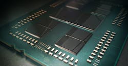
AMD’s EPYC “ROME” uses TSMC’s 7-nm transistor technology to double its performance per socket and quadruple its floating-point performance. Architectural advances for the Zen 2 cores include improved branch prediction, better instruction prefetch, an optimized instruction cache, and a larger op-cache. The floating-point support is now built around 256-bit data.
EPYC also supports runtime Secure Memory Encryption (SME) and Secure Encrypted Virtualization (SEC). With SME, data in RAM is encrypted and decrypted when inside the CPU. Data is encrypted before being written to RAM.
SME provides each VM with its own encryption keys. This allows an encrypted VM to be managed by a hypervisor that doesn’t have direct access to data within the VM. As with SME, the support is transparent to the operating systems and applications.
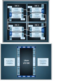
1. AMD’s “ROME” EPYC consists of a “chiplet” collection of 7-nm CPU cluster (top) and a 14-nm I/O cluster (bottom) tied together with a multi-die interposer.
I did mention more cores as being important, and this EPYC chip will have up to 64 of them. These are actually built from eight “chiplets” with eight cores each (Fig. 1). The I/O support is built using 14-nm technology. EPYC also has 128 PCI Express (PCIe) Gen 4 lanes, plus eight DDR4 memory channels to feed the cores.
Intel’s Cascade Lake packs in 48 cores built from a pair of 24-core chips in a multichip package connected together using Intel’s Ultra Path Interconnect (UPI). Its dozen DDR4 memory channels are designed to support Intel’s Optane DC persistent memory DIMMs in a hierarchical storage configuration (Fig. 2). A two-chip configuration connected by UPI provides 24 DDR4 memory channels. Versions of this Xeon family will also support Intel’s Omni Path Fabric. Current versions of Cascade Lake use PCIe Gen 3, but PCIe Gen 4 is on the roadmap.
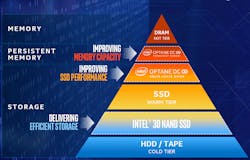
2. Intel’s server storage hierarchy includes Optane DC, which involves DIMMs connected to memory channels along with DRAM.
AVX-512, the 512-bit version of Intel’s Advanced Vector Extensions, will likely be a determining factor for many developers. It packs 32, double precision floating-point numbers in a 512-bit vector that can be processed in a clock cycle. The system includes a pair of fused-multiply-add (FMA) units.
Both AMD and Intel are tailoring their server support to address AI and ML. Intel’s Vector Neural Network Instructions (VNNI) that are part of the AVX-512 support represents just one example. These can be especially important in embedded applications where other ML accelerators may not be available.
ARM has been helping its partners push into the data-center space, offering solutions that challenge the entry-level and mid-range platforms. Its 7-nm “Ares” Neoverse infrastructure, which targets the cloud and IoT solutions, builds on the Cortex-A76 architecture. The challenge is that AMD and Intel are established players with solutions that include the high end.
GPUs in the Data Center
Though 64 cores are a lot for CPUs, the number pales in comparison to the amount of cores in a GPU. Granted, GPU cores are simpler and target more specific applications, but general-purpose GPUs (GPGPUs) are becoming more flexible. Programming platforms like OpenCL have pulled GPGPUs into the programming mainstream and they were the initial workhorses in the rise of AI/ML applications. They remain the preferred training platform in the cloud. NVIDIA and AMD are the main players when it comes to high-performance GPGPUs, with ARM, Imagination, and Intel providing integrated offerings that show up in CPU/GPU SoCs.
NVIDIA has taken the high ground when it comes to GPUs. Its NVLink connection is supported by its 16-port NVLink NVSwitch and Tesla V100 GPUs that have a half-dozen NVLink connections. This allows them to build the DGX2 (Fig. 3) with 12 NVSwitch chips and 16 GPUs that act like a single system in much the same fashion as a CPUs. It has 512 GB of HBM2 high bandwidth memory, 1.7 TB of system memory, and 32 TB of NVMe SSDs; a pair of Intel Xeon CPUs provide management support. The DGX2 is designed for the data center where multiple DGX2s are likely to reside side-by-side.
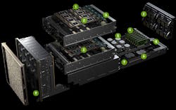
3. NVIDIA’s DGX2 combines (1) 16 TESLA V100 GPU modules with (2) a total of 512 GB of HBM2 memory using a (3) dozen NVSwitch chips. It also has (4) eight EDR InfiniBand or 100-Gb Ethernet ports, (5) a PCIe switch complex, (6) two Intel Xeon Platinum processors, (7) 1.7 TB of system memory, (8) dual 10/25-Gb Ethernet ports and (9) 30 TB of NVMe SSD storage.
The Tesla V100 GPU uses the Volta architecture that’s also found in the Jetson AGX Xavier. Targeting embedded applications, this single-chip solution incorporates multiple ARMv8 cores and accelerators, including two NVIDIA deep-learning accelerators (NVDLAs).
AMD’s Radeon Instinct MI60 compute card (Fig. 4) uses AMD’s Infinity Fabric, which can connect up to two GPU hives that consist of four MI60 GPUs in a single server. The MI60 is also built on 7-nm technology that takes of advantage of AMD’s Vega GPU architecture with 64 compute units and 4096 stream processors. The chip incorporates 32 GB of HBM2 memory with ECC. The HBM2 has a bandwidth of 1 TB/s. In addition, a x16 PCIe Gen 4 interface supports the ROCm Open Ecosystem. A single board delivers 59 TOPS of INT8, 29.5 TFLOPS of FP16, 14.7 TFLOPS of FP32 and 7.4 TFLOPS of FP64.
4. AMD’s Radeon Instinct MI60 compute card is based on AMD’s Vega GPU architecture.
The Instinct family includes the MI60, MI50, MI25, and M8. The M8 is a half-length card has only 4 GB of memory and foregoes the compute units to target embedded applications that need floating-point acceleration.
NVIDIA’s Volta and AMD’s Vega, like most GPGPUs these days, incorporate deep-learning support. This usually includes the ability to munch 8-bit integers (INT8) along with 16-, 32- and 64-bit floating point. The INT8 support is typically used with neural-network training and inference while floating point is used for more conventional computation.
FPGAs in the Data Center
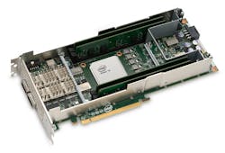
5. Intel’s PSG Stratix 10 employs a Stratix 10 FPGA based on the company’s Hyperflex FPGA architecture.
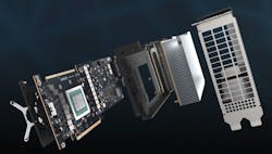
One of the biggest changes coming in the data center is the use of FPGAs like Intel’s PSG Stratix 10 (Fig. 5) and Xilinx’s Alveo (Fig. 6). Part of the change is due to hardware, but the biggest change is in the software.
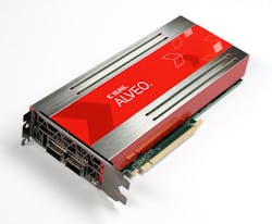
6. Xilinx’s Alveo U280 can deliver 24.5 INT8 TOPS and has one million LUTs.
The PSG Stratix 10 is a member of Intel’s Programmable Acceleration Card (PAC) series. It has an FPGA with 2.8 million logic elements, 32 GB of DDR4 using four memory channels, and x16 PCIe Gen 3. The Stratix 10 FPGA is based on Intel’s Hyperflex FPGA architecture using Intel’s 14-nm Tri-Gate process. It has a pair of QSFP28 network interface sockets.
Xilinx’s Alveo U280 is the top-end board with a 16-nm Xilinx UltraScale FPGA. It has 8 GB of HBMS2 memory with a 460-GB/s bandwidth. The boards have a x16 PCIe Gen 4 interface that supports CCIX. CCIX is a cache-coherent protocol that runs atop PCIe hardware in parallel with the PCIe protocol.
FPGA boards have been available for decades, although mostly for embedded applications. The tools for creating the IP that works with an FPGA have improved significantly, and it’s even possible to turn software written for frameworks like OpenCL directly into FPGA IP. Embedded developers typically handle the loading of this IP onto the FPGA, and it’s often tightly integrated with the application software.
Xilinx and Intel are adding a standard system software layer between the application and the hardware. This allows developers to treat the FPGA more like a black box with a standard API. Developers can build or buy the IP that’s used in the black, making the hardware more independent of the application.
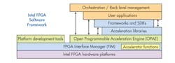
7. The Open Programmable Acceleration Engine (OPAE) runs on top of the FPGA Interface Manager (FIM) to manage Programmable Acceleration Cards (PACs).
For example, Intel’s Open Programmable Acceleration Engine (OPAE) runs on top of the FPGA Interface Manager (FIM) to manage its PAC FPGAs (Fig. 7). The software manages FPGA configuration and data movement to and from the FPGA and application. It needn’t be concerned with the hardware configuration as long as the IP fits in the FPGA available to the system. The OPAE is responsible for managing the use of the FPGAs in the system that can change over time as new applications are started.
Other major factors are affecting the data center and embedded servers from persistent memory technology to the upcoming PCIe Gen 5 and CCIX. But that’s for another article.

About the Author

William G. Wong
Senior Content Director - Electronic Design and Microwaves & RF
I am Editor of Electronic Design focusing on embedded, software, and systems. As Senior Content Director, I also manage Microwaves & RF and I work with a great team of editors to provide engineers, programmers, developers and technical managers with interesting and useful articles and videos on a regular basis. Check out our free newsletters to see the latest content.
You can send press releases for new products for possible coverage on the website. I am also interested in receiving contributed articles for publishing on our website. Use our template and send to me along with a signed release form.
Check out my blog, AltEmbedded on Electronic Design, as well as his latest articles on this site that are listed below.
You can visit my social media via these links:
- AltEmbedded on Electronic Design
- Bill Wong on Facebook
- @AltEmbedded on Twitter
- Bill Wong on LinkedIn
I earned a Bachelor of Electrical Engineering at the Georgia Institute of Technology and a Masters in Computer Science from Rutgers University. I still do a bit of programming using everything from C and C++ to Rust and Ada/SPARK. I do a bit of PHP programming for Drupal websites. I have posted a few Drupal modules.
I still get a hand on software and electronic hardware. Some of this can be found on our Kit Close-Up video series. You can also see me on many of our TechXchange Talk videos. I am interested in a range of projects from robotics to artificial intelligence.
Comment About the Article
To join the conversation, and become an exclusive member of Electronic Design, create an account today!

Leaders relevant to this article: