What’s the Difference Between 2- and 4-Layer PCBs?
Download this article in PDF format.
Multi-layered printed circuit boards (PCBs) are typically preferred because they offer high signal intensity. Of all the multi-layered types, the 2-layer PCB is the most common, as it can accommodate interconnects on both sides. Depending on the desired level of complexity, PCBs can range from two to eight layers—every increment means the addition of two more layers.
It comes as no surprise that differences exist among these layered PCB types. This article is devoted specifically to understanding the differences between 2- and 4-layer PCBs.
Comparing Stackups
The 2-layer PCB stackup can be clearly demarcated. Layer 1, or the top layer, is described as a signal layer. The 0.0014-in.-thick layer is made of copper material; the copper amounts to about 1 oz. These parameters are valid for a board whose final thickness is 0.062 in., ±10%. If the PCB manufacturer plans to make custom PCBs, then these values may differ in accordance with the desired parameters.
The 4-layer PCB stackup, on the other hand, is quite elaborate. Two inner layers, inner layer 1 and 2, are sandwiched between the top and bottom layers. From top to bottom, the 4-layer PCB stackup goes something like this:
The top, i.e. the signal layer (0.0014 in. width) is followed by a prepreg layer with a thickness of 0.0091 in. and dielectric constant of 4.2. The top layer is copper material. The prepreg layer is followed by inner layer 1 (0.0014 in.), referred to as the plane. A core sublayer is part of inner layer 1, which has a width of 0.037 in. This is followed by inner layer 2, which is another plane layer made with 1 oz. copper and is 0.0014 in. thick. Another prepreg sublayer constituting two sheets that are 0.0091 in. thick forms part of inner layer 2. The final layer, the bottom layer, is also 0.0014 in. thick, and is a signal layer as well. Interconnects are soldered and placed on the top and bottom layers.
Comparing Design
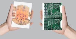
The 2-layer PCB’s design (Fig. 1) provides more surface area for housing a conductor pattern. It can safely be said that the surface is two times larger than that of a single-layer PCB. Vias are employed to create electrical connections that enable the routing of the traces so that they reach the opposite side of the board.
1. This is an example of a 2-layer PCB design (Source: Elecrow)
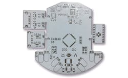
On the other hand, as mentioned earlier, even more surface area is available for traces in a 4-layer PCB design (Fig. 2). Creating the 4-layer PCB design involves a prepreg layer that bonds two or more double-sided boards by applying heat and pressure. The number of distinct conductor patterns generated equates the final number of layers. Prepreg also provides dielectric between the layers.
2. Shown is an example of a typical 4-layer PCB design. (Source: Elecrow)
Comparing Functionality
If the microstrip traces comprising a ground plane will be employed, the 2-layer PCB delivers more functionality as there are no propagation delays or other issues. Nonetheless, a 4-layer PCB design consisting of ground and VCC plane layers and two signal layers is more preferable. This design does struggle with impedance and propagation delays, though.
Comparing Cost
When it comes to cost, it’s no surprise that the 4-layer PCB is more expensive due to complexity of design and higher sensitivity. The superior quality of signals, achieved by reducing distortion and propagation levels, is also a factor 4-layer PCB cost. Because of the higher levels of signal integrity and reduced interference levels, more manufacturers are deciding to invest in 4-layer PCBs.
Comparing the Making of Prototypes
The challenge of achieving a perfect PCB can be easily met through the prototyping process. Though a typical 4-layer PCB prototype is a bit more complex than a 2-layer version, automated software like Gerber is available to help accelerate prototype production. The software comes with a number of preset parameters, such as board thickness, hole thickness, minimum pitch, board finishing, etc. Going this route also simplifies the creation of custom PCBs, whether 2 layer or 4 layer.
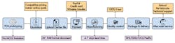
3. This is the typical PCB prototyping fulfillment process. (Source: Elecrow)
Outsourcing to a manufacturer that provides PCB prototyping services can also be a cost-effective way to obtain customized PCB prototypes. For instance, Elecrow’s PCB prototyping service, backed up by the strong production lines, has support for instant online quotes and uploading of Gerber files. It can cut lead time down to three days, no matter where the location. PCB rush services are also available for high-priority projects. Figure 3 illustrates the typical PCB prototyping service process.

About the Author
Yi Tang
PCB Market Researcher
Elecrow, located in Shenzhen, China, is a company devoted to the open-source hardware industry. Its online store offers open-source hardware products related to Arduino, Raspberry Pi, 3D printing, and other electronic components, and provides one-stop OEM/ODM solutions from original prototyping to batch manufacturing (circuit design, PCB prototyping, assembly).
Comment About the Article
To join the conversation, and become an exclusive member of Electronic Design, create an account today!

Leaders relevant to this article: