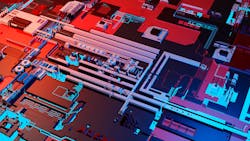
Reverse Engineering a Printed Circuit Board
What you’ll learn:
- What is reverse engineering?
- Tools used to reverse engineer a PCB.
- Specifics about de-layering
Printed-circuit-board (PCB) reverse engineering is a method of analyzing and understanding the design principles behind an existing electronic product. It’s a process of dismantling and studying a PCB to gain knowledge of its design and operation. The process also helps in reproducing the PCB at a lower cost or with better features. Furthermore, documents can be generated during this method for future reference.
In the semiconductor industry, reverse engineering provides complete process information and material descriptions. It can be classified into four types. Product teardown is the basic type of reverse engineering in the electronics domain. It’s basically the opposite of what’s done in PCB assembly. Here, the focus is to know only the components used in the design.
In system-level evaluation, the effort is to understand the operation, functionality, and interconnection details of the circuit. Apparatus like logic analyzers and oscilloscopes are used to know the signal paths and timing characteristics. The next level is the process analysis, which involves study of the material composition. Finally, the circuit extraction includes de-layering the PCB to generate schematics and netlists.
As reverse engineering is usually applied to old PCB designs, knowing the process can assist in finding a cost-effective alternate for an obsolete component present in the circuit. It can help in porting the old design to the latest platforms for functional upgrades. In addition, it can extract the design documents for future reference. Recently, though, this technique is used to identify and understand the features of a competitor’s product as well.
Reverse-Engineering Procedure
The process of reverse engineering a PCB mainly includes the following steps:
- Creating circuit images by drawing, scanning, or taking photographs.
- Editing and uploading the images in suitable reverse-engineering software.
- Replicating the layout design for each layer of the PCB.
- Generating the circuit schematics using an appropriate tool.
To start the process of reverse engineering, a sample PCB (bare board or populated) is required. In the reverse-engineering method, the PCB is first examined on the external layers for mounted components, connectors, and traces. Later, the PCB is de-layered to analyze the traces and vias in the internal layers. The detailed process of reverse engineering a PCB is discussed below.
The PCB image must be captured by scanning or taking a photograph. The scanning machine or the camera should have high resolution. The image should be captured in a well-lighted space on a dark background. This is important if the PCB has a complex design. If it’s a simple design, then the circuit can be handwritten with the exact dimensions of the PCB. There may be a further need to edit the image to meet the requirements of the software used in the next step.
In manual PCB reverse engineering, identifying the components, preparing the bill of materials (BOM), gathering the technical details of the components, and analyzing the signals are done physically. This is a tedious process and needs prior knowledge and expertise.
However, in the automatic reverse-engineering method, machine vision equipment detects the components and the datasheets are obtained via the internet. PCB reverse-engineering software is available with features like schematic drawing, signal simulation for analog and digital circuits, etc. Using high-resolution PCB images, the IC part numbers also can be extracted.
Software Tools
Several software tools are available to generate the schematics and the PCB layout. A 3D layout generated from the reverse-engineering software can provide vital information pertaining to the PCB, such as the electromechanical field distribution, trace mapping, and layer stack-up details. But the image used by the software to develop the schematics would require lots of editing and patience.
Multiple editing strategies can be used for each PCB layer. It may include methods like highlighting the component pads and holes in the image by painting to enhance the visibility. To increase the efficiency of the auto tracer, it’s necessary to mark holes, remove trackpads to avoid loops, and clean the tracks. The generated 2D assembly drawing represents the schematics of the PCB.
De-Layering
In the case of multilayer PCBs, the reverse-engineering process involves the removal of solder masks followed by de-layering of the PCB to obtain the images of internal layers. If the multilayer PCB fabrication process is done efficiently, you may face some troubles while reverse engineering it.
There are several methods of PCB de-layering, such as the sandpaper method, x-ray, surface grinding, etc. After obtaining the image of each PCB layer, they’re arranged cautiously to avoid any misalignment. The schematics and the layout obtained from the reverse-engineering process can enable many applications like redesigning the product for RoHS compliance, migrating from through-hole to surface-mount devices, replacing the obsolete components, debugging any failure in the circuit, etc.
The traditional reverse-engineering method is based on a destructive process of de-layering the PCB for imaging. This process is time-consuming and error-prone. Also, the PCB is damaged and can’t be reused. But a new reverse-engineering technique is based on x-ray tomography, which takes a shorter duration for the evaluation process. X-ray tomography enables the extraction of required data of traces, vias, and holes on the PCB layers by using algorithms.
Pros and Cons
PCB reverse engineering has both advantages and disadvantages in the electronics industry. It serves as a validating tool for the quality and integrity of electronic devices. In systems and infrastructures like automotive and aerospace equipment using PCB designs that are decades old, there may not be any reference documents for debugging or for maintenance purposes. Replacing such setups can be expensive and reverse engineering may be the best solution in such situations.
On the other hand, if reverse engineering is applied on the PCBs used in defense systems, then national security may be compromised. Reverse engineering also could assist piracy or cloning of PCB products. To avoid any such negative applications, experts are working on including countermeasures. Some PCB designers erase the IC markings to hide the manufacturing part numbers of the major chips used in the design.
Sometimes, the complexities involved in the PCB reverse-engineering process can be too challenging and thus the need arises for an experienced reverse-engineering service provider. They can provide specific services like building a “known parts” database for checking counterfeit components, gathering competitive information for preparing new products, and identifying any patent infringements along with the primary process of PCB circuit extraction.
About the Author
Suresh Patel
Sales Engineer, Mer-Mar Electronics
Suresh Patel has worked as a Sales Engineer and held other management roles at Mer-Mar. He brings 25 years of experience in printed-circuit-board sales and technical client service and managing business.
Comment About the Article
To join the conversation, and become an exclusive member of Electronic Design, create an account today!

Leaders relevant to this article: