Download this article in PDF format.
Wireless technology is a large part of modern communications, requiring more bandwidth for growing numbers of users and functions. Much of the promise of 5G wireless cellular networks hinges on optimum use of available bandwidth, especially at millimeter-wave (mmWave) frequencies.
Effective radio networks will require efficient power amplification and NXP Semiconductors has recognized that a single semiconductor technology may not be enough for 5G. The semiconductor innovator is developing discrete and integrated device solutions for 5G based on three different in-house technologies: silicon (Si) LDMOS, gallium-nitride (GaN), and silicon-germanium (SiGe) processes. In addition to transistors and amplifiers, the firm has developed integrated multiple-input, multiple-output (MIMO) integrated antenna modules as part of efforts to reduce the size and costs of future wireless cellular base stations.
NXP is perhaps best known as a global supplier of high-power Si LDMOS transistors and amplifiers, widely used as the active analog power devices in cellular communications infrastructure equipment, such as base-station transmitters. With an LDMOS device lineup that includes transistors running on supplies from +7.5 to +65 V dc and delivering RF/microwave output power levels from 1 to 1800 W at frequencies from 1 MHz to 5 GHz, NXP has supported the various generations of wireless cellular equipment in addition to applications in aerospace, broadcast, medical, and military systems.
This is hardly a “single semiconductor process” supplier, though—it draws from expertise in multiple semiconductor processes. At the recent 2019 IEEE International Microwave Symposium (IMS) in Boston, Mass., the firm’s representatives displayed packaged devices currently serving 3G and 4G Long Term Evolution (LTE) wireless systems—devices that are also expected to assist the expansion of remote radio heads (RRHs) in 5G systems. In keeping with NXP’s approach of matching the semiconductor technology to the application, the devices on display were based on both Si LDMOS and GaN technologies.
One Si LDMOS device, model A3T21H456W23S, was not new for that exhibition, although its performance is noteworthy. The device, a member of the company’s Airfast product line, can produce healthy continuous-wave (CW) and peak output power levels from a compact flange package. The N-channel enhancement-mode LDMOS transistor runs on +30 V dc (with quiescent current of 800 mA) and is capable of 87 W CW output power and 562 W peak output power from 2110 to 2200 MHz.
Perhaps what is surprising about the asymmetrical Doherty device is the package: an air-cavity plastic package capable of safely dissipating excess heat for reliable and long transistor operating life. The RoHS-compliant (lead-free) device can withstand high output VSWR (load-mismatch) conditions and is well-suited for applications requiring wide instantaneous bandwidth.
The power transistor features a wide negative-gate-source-voltage range for improved Class C operation and high efficiency; typical drain efficiency is 49.5%. Typical power gain is 14.8 dB at 2110 MHz when tested in a Doherty fixture, with gain rising to 15.3 dB at 2140 MHz. And typical peak-to-average power ratio (PAR) at both frequencies is 8 dB.
The plastic-packaged transistor achieves a typical 3-dB compression point of +56.8 dBm when evaluated with a single-carrier wideband-code-division-multiple-access (W-CDMA) test signal, with typical adjacent-channel power ratio (ACPR) of −30.3 dBc. For many small-cell base-station applications, this transistor will provide the final-stage output power in a multiple-stage amplifier configuration.
Give It the GaN
To show what it could do in GaN at higher frequencies, the firm also displayed its +48-V dc A3G26H200W17S GaN power transistor for use at 2496 to 2690 MHz. The GaN transistor delivers 30 W CW power and 200 W peak output power over that frequency range. It’s also an asymmetrical Doherty device like the A3T21H456W23S, but unlike the LDMOS device, is supplied in an air-cavity ceramic package rather than a plastic package.
The GaN power transistor, which is well-suited for final-stage amplification in small cells, features 56% typical power-added efficiency. It delivers 14.3 dB power gain at 2496 MHz with 13.8 dB power gain at 2690 MHz. The typical PAR at 2496 MHz is 8.2 dB with a typical ACPR of −30 dBc. The typical PAR at 2690 MHz is 7.6 dB with typical ACPR of −36.1 dBc.
As with the lower-frequency LDMOS device, this GaN transistor can function as part of a small-cell, base-station amplification lineup completed by other NXP transistors based on different semiconductor process technologies. For example, the GaN device would serve as the final stage in an amplification lineup that would include a MMG3014N predriver device and a A2125D025N driver stage.
In keeping with using different semiconductor technologies for different functions, the MMG3014N is a broadband amplifier based on an indium-gallium-arsenide (InGaP) heterojunction-bipolar-transistor (HBT) semiconductor process. It’s also supplied in a plastic package—an SOT-89 surface-mount housing—but this is a small-signal device meant to boost low-level signals prior to power amplification by larger, higher-power semiconductors. The amplifier provides generous gain over a range of 40 to 4000 MHz, with 19.5-dB small-signal gain at 900 MHz.
The driver stage in the three-device cellular amplification lineup, the model A2125D025N, returns to Si LDMOS technology for higher power over a broad frequency range, 2100 to 2900 MHz. It’s an integrated circuit (IC) with multiple transistor stages and on-chip impedance matching (to 50 Ω) that runs on supplies of +26 to +32 V dc. Supplied in a multipin plastic package, the IC is capable of 31.7-dB typical power gain or more across the full frequency range, with PAE of 19% or more across that frequency range. The typical CW output power at 1-dB compression is 24 W.
Terminating Tubes
In addition to supporting a wide range of traditional applications with its various semiconductor technologies, NXP introduced a GaN-on-silicon-carbide (GaN-on-SiC) power device at the IMS exhibition. It’s the company’s first such semiconductor device for RF energy applications in the industrial-scientific-medical (ISM) band from 2400 to 2500 MHz.
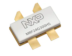
Designed as a solid-state replacement for high-power magnetron vacuum tubes in such applications as heating and welding systems at 2450 MHz, the MRF24G300HS (Fig. 1) leverages its extremely high efficiency and the high conductivity of SiC to provide high CW output power levels within such a small package. The transistor has a nominal operating temperature range of 0 to +55°C. It’s available as model MRF24G300H in an air-cavity ceramic package with mounting flanges and as model MRF24G300HS in a package without mounting flanges.
1. Model MRF24G300HS is a high-power GaN-on-SiC transistor developed for CW and long-pulse application from 2400 to 2500 MHz, and as a solid-state replacement for magnetrons at 2.45 GHz in heating and welding systems. (Courtesy of NXP Semiconductors)
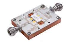
When tested in a MRF24G300HS reference circuit (Fig. 2) with drain voltage of +48 V dc and gate-source voltage of −5 V dc, and soldered to a heatsink for good thermal flow, the transistor offers typical measured power gain of 15.3 dB at 2400 MHz and 14.9 dB at 2500 MHz (see table). Such high-power gain transforms a 10-W CW input signal at 2400 MHz to a 336-W CW output signal and a 10-W CW input signal at 2500 MHz to a 307-W CW output signal.
2. This reference circuit was used to characterize a high-power GaN-on-SiC transistor meant as a solid-state replacement for magnetrons in ISM RF energy applications at 2400 to 2500 MHz. (Courtesy of NXP Semiconductors)
Typical power-added efficiency (PAE) for the device is 70.4% or better across the full 100-MHz bandwidth, reaching more than 74% at 2500 MHz. It can be used in single-ended or push-pull amplifier configurations and has been characterized for CW operation as well as with short and long (as long as several seconds) pulses.
In addition to its ability to produce high power in much smaller footprints than magnetrons, power transistors such as the model MRF24G300HS promise longer operating lifetimes than tubes with much more flexibility than magnetrons. That’s due to bias control, which makes it possible to dynamically adjust the power, frequency, and phase of the output signal energy of the transistor for optimum heating/welding results.
The high-power density of GaN semiconductor materials makes them well-equipped for RF energy applications, even compared to Si LDMOS technology: The 73% drain efficiency measured for the MRF24G300HS transistor at 2.45 GHz is five percentage points higher in PAE than the most advanced Si LDMOS devices at the same frequency. In addition, the GaN-on-SiC transistor exhibits high output impedance compared to LDMOS devices, to enable broadband impedance matching compared to LDMOS devices, The MRF24G300HS also features simplified gate biasing to remove some of the mystery from starting the power-up sequence for GaN transistors.
Handling Higher Frequencies
These LDMOS and GaN devices will provide usable transmit power levels within frequency bands currently used for 3G and 4G systems as well as some lower-frequency bands of 5G from about 600 MHz to 6 GHz. But what about handling the 5G signals reaching into mmWave frequency bands, such as from 26 to 29 GHz and 37 to 40 GHz?
NXP is exploring the use of massive multiple-input, multiple-output (mMIMO) active-antenna arrays for use in RRHs of 5G small cells utilizing multifunction (such as switching and amplification) multichip modules (MCMs) in miniature surface-mount packages, including packages measuring 10 × 6 mm and 4 × 3 mm. The MCMs are based on the firm’s various semiconductor technologies, such as Si LDMOS and GaN. In addition, the modules include matching to 50 Ω to simplify integration in mMIMO antenna systems.
These antenna systems are being developed with 16 to 64 transmit and receive paths/antenna elements in a single active antenna constructed with antenna elements, filters, switches, antenna modules, and impedance matching under cloud-based automated control. Such mMIMO antenna systems have already been applied in time-division-multiple-access (TDMA) formats and are expected to move to frequency-division-multiple-access (FDMA) configurations with the design and construction of 5G infrastructure equipment.
In quest of semiconductor solutions at 5G mmWave frequencies, such as 26 through 40 GHz, NXP refers to its silicon-germanium (SiGe) semiconductor technology as a “sweet spot” for low cost and power consumption compared to other semiconductor technologies. The semiconductor technology has long held the promise of low-noise, high-gain capabilities in heterojunction bipolar transistors (HBTs) for microwave and mmWave frequencies while producing discrete devices and ICs on low-cost silicon semiconductor substrates. If 5G grows as expected, SiGe semiconductor process technology could reach high mass-production numbers in devices for predriver, driver, and output stages in potentially millions of RRHs and small cells.
NXP Semiconductors, 411 E. Plumeria Dr., San Jose, CA 95134; (408) 518-5291.
About the Author
Jack Browne
Contributing Editor
Jack Browne, Technical Contributor, has worked in technical publishing for over 30 years. He managed the content and production of three technical journals while at the American Institute of Physics, including Medical Physics and the Journal of Vacuum Science & Technology. He has been a Publisher and Editor for Penton Media, started the firm’s Wireless Symposium & Exhibition trade show in 1993, and currently serves as Technical Contributor for that company's Microwaves & RF magazine. Browne, who holds a BS in Mathematics from City College of New York and BA degrees in English and Philosophy from Fordham University, is a member of the IEEE.
Voice Your Opinion!
To join the conversation, and become an exclusive member of Electronic Design, create an account today!

Leaders relevant to this article:


