Power Management, Chapter 7: Voltage Regulator ICs

This articles is part of the Power Management Series in the Power Management section of our Series Library.
Download this article as a .PDF eBook.
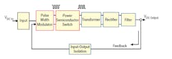
Virtually all power supplies employ semiconductors to provide a regulated output voltage. If the supply has an ac input, it is rectified to be a dc voltage. A power converter IC accepts the dc input and produces a dc output or controls external power output semiconductor switches to produce a dc output. It is a voltage regulator when its output voltage is fed back to a circuit that causes the voltage remains constant. If the output voltage tends to rise or fall, the feedback causes the output to remain the same.
The power converter can operate either as a switch-mode or linear circuit. In a linear configuration, the controlling transistor always dissipates power, which can be minimized by using low dropout regulators (LDOs) that regulate properly even when there is a relatively low voltage differential between their input and output. LDO ICs have simpler circuits than their switch-mode cousins and produce less noise (no switching), but are limited by their current-handling and power dissipation capability. Some LDO ICs are specified at about 200mA and others can handle up to about 1A.
Efficiency of the LDO ICs may be 40-60%, whereas the switch-mode ICs can exhibit up to 95% efficiency. Switch-mode topologies are the primary approach for embedded systems, but LDOs also find use in some applications.
Low Dropout (LDO) Linear Regulator
LDO linear regulators are usually employed in systems that require a low-noise power source instead of a switching regulator that might upset the system. LDOs also find use in applications where the regulator must maintain regulation with small differences between the input supply voltage and output load voltage, such as battery-powered systems. Their low dropout voltage and low quiescent current make them a good fit for portable and wireless applications. LDOs with an on-chip power MOSFET or bipolar transistor typically provide outputs in the 50 to 500mA range.
An LDO voltage regulator operates in the linear region with the topology shown in Fig. 7-1. As a basic voltage regulator, its main components are a series pass transistor (bipolar transistor or MOSFET), differential error amplifier, and precise voltage reference.
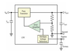
7-1. In the basic LDO, one input to the differential error amplifier, set by resistors R1 and R2, monitors a percentage of the output voltage. The other error amplifier input is a stable voltage reference (VREF). If the output voltage increases relative to VREF, the differential error amplifier changes the pass-transistor’s output to maintain a constant output load voltage (VOUT).
Key operational factors for an LDO are its dropout voltage, power-supply rejection ratio (PSRR), and output noise. Low dropout refers to the difference between the input and output voltages that allow the IC to regulate the output load voltage. That is, an LDO can regulate the output load voltage until its input and output approach each other at the dropout voltage. Ideally, the dropout voltage should be as low as possible to minimize power dissipation and maximize efficiency. Typically, dropout is considered to be reached when the output voltage has dropped to 100mV below its nominal value. The load current and pass transistor temperature affect the dropout voltage.
An LDO’s internal voltage reference is a potential noise source, usually specified as microvolts RMS over a specific bandwidth, such as 30 µV RMS from 1 to 100 kHz. This low-level noise causes fewer problems than the switching transients and harmonics from a switch-mode converter. In Fig. 7-1, the LDO has a (voltage-reference) bypass pin to filter reference voltage noise with a capacitor to ground. Adding the datasheet-specified input, output, and bypass capacitors usually results in a non-problematic noise level.
Among their operational considerations are the type and range of the applied input voltage, required output voltage, maximum load current, minimum dropout voltage, quiescent current, power dissipation, and shutdown current.
Controlling the LDO’s frequency compensation loop to include the load capacitor reduces sensitivity to the capacitor’s ESR (equivalent series resistance), which allows a stable LDO with good quality capacitors of any type. In addition, output capacitor placement should be as close as possible to the output.
Additional features in some LDOs are:
- An enable input that allows external control of LDO turn-on and turn-off.
- Soft-start that limits inrush current and controls output voltage rise time during power-up.
- A bypass pin that allows an external capacitor to reduce reference voltage noise.
- An error output that indicates if the output is going out of regulation.
- Thermal shutdown that turns the LDO off if its temperature exceeds the specified amount.
- Overcurrent protection (OCP) that limits the LDO’s output current and power dissipation.
LT3042
The LT3042 from Linear Technology is a low dropout (LDO) linear regulator that uses a unique architecture to minimize noise effects and optimize Power-Supply Ripple Rejection (PSRR).
PSRR describes how well a circuit rejects ripple, injected at its input. The ripple can be either from the input supply such as a 50Hz/60Hz supply ripple, switching ripple from a DC/DC converter, or ripple due to the sharing of an input supply with other circuits.
For LDOs, PSRR is a function of the regulated output voltage ripple compared to the input voltage ripple over a given frequency range (typically10Hz to 1MHz), expressed in decibels (dB). It can be an important factor when an LDO powers analog circuits because a low PSRR may allow output ripple to affect other circuits.
Low-ESR output capacitors and added reference voltage bypass capacitors improve the PSRR performance. Battery-based systems should employ LDOs that maintain high PSRR at low battery voltages.
The LT3042 shown in the simplified schematic of Fig. 7-2 is an LDO that reduces noise and increases PSRR. Rather than a voltage reference used by most traditional linear regulators, the LT3042 uses a current reference that operates with a typical noise current level of 20pA/√Hz (6nARMS over a 10Hz to 100kHz bandwidth).
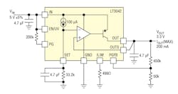
7-2. The LT3042 is an LDO that uses a unique architecture to minimize noise effects and optimize Power Supply Ripple Rejection (PSRR).
The current source is followed by a high performance rail-to-rail voltage buffer, allowing it to be easily paralleled to further reduce noise, increase output current and spread heat on a PCB. Paralleling multiple LT3042s further reduces noise by a factor of √N, where N is the number of parallel circuits.
LT3080
Linear Technology’s LT3080 is a unique, 1.1A LDO that you can paralleled to increase output current or spread heat in surface-mounted boards (Fig. 7-3). This IC brings out the collector of the pass transistor to allow low dropout operation—down to 350 mV—when used with multiple supplies. Protection features include short-circuit and safe operating area protection, as well as thermal shutdown.
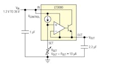
7-3. The LT3080 can program output voltage to any level between zero and 36V.
A key feature of the LT3080 is the capability to supply a wide output voltage range. By using a reference current through a single resistor, the output voltage is programmed to any level between zero and 36V. It is stable with 2.2μF of capacitance on the output, and can use small ceramic capacitors that do not require additional ESR, unlike other regulators.
The LT3080 is especially well suited to applications needing multiple rails. Its architecture adjusts down to zero with a single resistor handling modern low-voltage digital ICs as well as allowing easy parallel operation and thermal management without heat sinks. Adjusting to “zero” output allows shutting off the powered circuitry and when the input is pre-regulated—such as a 5V or 3.3V input supply—external resistors can help spread the heat.
A precision “0” TC 10μA internal current source connects to the non-inverting input of its power operational amplifier, which provides a low-impedance buffered output to the voltage on the non-inverting input. A single resistor from the non-inverting input to ground sets the output voltage; setting this resistor to zero produces zero output. Any output voltage can be obtained from zero up to the maximum defined by the input power supply.
Use of a true current source allows the regulator to exhibit gain and frequency response independent of the positive input impedance. Older adjustable regulators change their loop gain with output voltage and change bandwidth when bypassing their adjustment pin. For the LT3080, the loop gain is unchanged by changing the output voltage or bypassing. Output regulation is not fixed at a percentage of the output voltage but is a fixed fraction of millivolts. Use of a true current source allows all the gain in the buffer amplifier to provide regulation and none of that gain is needed to boost the reference to a higher output voltage.
The IC can operate in two modes. One is the three-terminal mode that connects the control pin to the power input pin, which limits it to 1.35V dropout. Alternatively, you can connect the “control” pin to a higher voltage and the power IN pin to a lower voltage, resulting in 350mV dropout on the IN pin and minimizing the power dissipation. This allows a 1.1A supply regulating from 2.5VIN to 1.8VOUT or 1.8VIN to 1.2VOUT with low dissipation.
Switch-Mode ICs
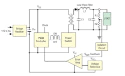
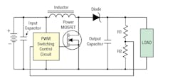
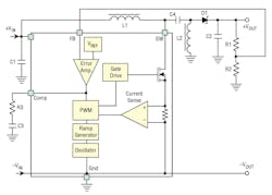
Figure 7-4 shows a simplified PWM controller employed with a switch-mode converter. In operation, a fraction of the dc output voltage feeds back to the error amplifier, which causes the comparator to control the PWM ON and OFF times. Figure 7-4 shows how the PWM pulse width changes for different percentages of ON and OFF times. The longer the ON time, the higher the rectified dc output voltage. Output voltage regulation is maintained if the power MOSFET’s filtered output tends to change, if this occurs feedback adjusts the PWM duty cycle to keep the output voltage at the desired level.
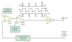
7-4. A PWM controller produces square waves of different widths dependent on the out voltage feedback.
To generate the PWM signal, the error amplifier accepts the feedback signal input and a stable voltage reference to produce an output related to the difference of the two inputs. The comparator compares the error amplifier’s output voltage with the ramp (sawtooth) from the oscillator, producing a modulated pulse width. The comparator output is applied to the switching logic, whose output goes to the output driver for the external power MOSFET. The switching logic provides the capability to enable or disable the PWM signal applied to the power MOSFET.
Most PWM controller ICs provide current limiting protection by sensing the output current. If the current sense input exceeds a specific threshold, it terminates the present cycle (cycle-by-cycle current limit).
Circuit layout is critical when using a current sense resistor, which must be a low inductance type. Locate the current sense filter capacitor very close to and connected directly to the PWM IC pin. Also, all the noise-sensitive low-power ground connections should be connected together near the IC GND and a single connection should be made to the power ground (sense resistor ground point).
In most PWM controller ICs, a single external resistor or capacitor sets the oscillator frequency. To set a desired oscillator frequency, use the equation in the controller datasheet to calculate the resistor value.
Some PWM converters include the ability to synchronize the oscillator to an external clock with a frequency that is either higher or lower than the frequency of the internal oscillator. If there is no requirement for synchronization, connect the sync pin to GND to prevent noise interference.
Because the PWM IC is a part of feedback circuit, the input to the error amplifier must employ a frequency compensation network to ensure system stability.
A typical power converter accepts a dc input, converts it to the switching frequency and then rectifies it to produce the dc output. A portion of its dc output is compared with a voltage reference (VREF) and controls the PWM. If the output voltage tends to increase, the voltage fed back to the PWM circuit reduces its duty cycle, causing its output to reduce and maintain the proper regulated voltage. Conversely, if the output voltage tends to go down, the feedback causes the power-switch duty cycle to increase, keeping the regulated output at its proper voltage.
Typically, the power semiconductor switch turns on and off at a frequency that may range from 100kHz to 1MHz, depending on the IC type. Switching frequency determines the physical size and value of filter inductors, capacitors, and transformers. The higher the switching frequency, the smaller the physical size and component value. To optimize efficiency, magnetic core material for the inductor and transformer should be consistent with the switching frequency. That is, the transformer/inductor core material should be chosen to operate efficiently at the switching frequency.
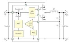
Figure 7-5 shows a simplified diagram of a switch-mode voltage regulator. Switch-mode dc-dc converters require a means to vary their output voltage in response to changes in their load. One approach is to use pulse-width modulation (PWM) that controls the input to the associated power switch. The PWM signal consists of two values, ON and OFF. A low-pass filter connected to the output of the power switch provides a voltage proportional to the ON and OFF times of the PWM controller.
7-5. Switch-mode converter uses pulse width modulator to control regulation
There are two types of switch-mode converters: isolated and non-isolated, which depends on whether there is a direct dc path from the input to the output. An isolated converter employs a transformer to provide isolation between the input and output voltage (Fig. 7-6).
7-6. Isolated switch-mode converter employs a transformer for isolation.
The non-isolated converter usually employs an inductor and there is no voltage isolation between the input and output (Fig. 7-7). For the vast majority of applications, non-isolated converters are appropriate. However, some applications require isolation between the input and output voltages. An advantage of the transformer-based converter is that it has the ability to easily produce multiple output voltages, whereas the inductor-based converter provides only one output.
7-7. Non-isolated switch-mode converter.
Circuit Topologies
There are two basic IC topologies employed in dc power converters. If the output is lower than the input voltage, the IC is said to be a step-down, or buck converter. If the output is higher than the input voltage, the IC is said to be a step-up, or boost converter.
In its basic circuit (Fig. 7-8), the buck regulator accepts a dc input, converts it to a PWM (pulse-width modulator) switching frequency that controls the output of the power MOSFET (Q1). An external rectifier, inductor, and output capacitor produce the regulated dc output. The regulator IC compares a portion of the rectified dc output with a voltage reference (VREF) and varies the PWM duty cycle to maintain a constant dc output voltage. If the output voltage tends to increase, the PWM reduces its duty cycle causing the output to reduce and keeping the regulated output at its proper voltage. Conversely, if the output voltage tends to go down, the feedback causes the PWM duty cycle to increase and maintain the regulated output.
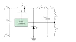
7.8. Basic buck converter; inductor always “bucks” or acts against the input voltage.
The buck, or step-down regulator topology has advantages of simplicity and low cost. However, it has a limited power range and its direct dc path from input to output can pose a problem if there is a shorted power switch.
LT8602
The LT8602 from Linear Technology is a constant-frequency, current-mode, monolithic buck-switching regulator with four output channels (Fig. 7-9). Two are high-voltage channels with a 3V to 42V input and the other two are low-voltage channels with a 2.6V to 5.5V input.
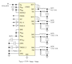
7-9. LT8602 Quad buck converter has two high-voltage channels with a 3V to 42V input and the other two are low-voltage channels with a 2.6V to 5.5V input.
The IC employs a single oscillator that generates two clock (CLK) signals 180 deg. out of phase. Channels 1 and 3 operate on CLK1, while channels 2 and 4 operate on CLK2. A buck regulator only draws input current during the top switch on cycle, so multiphase operation cuts peak input current and doubles the input current frequency. This reduces both input current ripple and the required input capacitance.
Each high-voltage (HV) channel is a synchronous buck regulator that operates from its own PVIN pin. The internal top-power MOSFET turns on at the beginning of each oscillator cycle, and turns off when the current flowing through the top MOSFET reaches a level determined by its error amplifier. The error amplifier measures the output voltage through an external resistor divider tied to the FB pin to control the peak current in the top switch.
While the top MOSFET is off, the bottom MOSFET is turned on for the remainder of the oscillator cycle or until the inductor current starts to reverse. If overload conditions result in more than 2A (Ch 1) or 3.3A (Ch 2) flowing through the bottom switch, the next clock cycle will be delayed until switch current returns to a lower, safe level.
High-voltage channels have Track/Soft-Start Inputs (TRKSS1, TRKSS2). When this pin is below 1V, the converter regulates the FB pin to the TRKSS voltage instead of the internal reference. The TRKSS pin has a 2.4μA pull-up current. The TRKSS pin can also be used to allow the output to track another regulator, either the other HV channel or an external regulator.
As shown in the simplified inductive-boost dc-dc converter circuit (Fig. 7-10), turning on the power MOSFET causes current to build up through the inductor. Turning off the power MOSFET forces current through the diode to the output capacitor. Multiple switching cycles build the output capacitor voltage due to the charge it stores from the inductor current. The result is an output voltage higher than the input.
7-11. LTC3124 application circuit employs an external resistive voltage divider from VOUT to FB to SGND to program the output from 2.5V to 15V.
Use of two phases equally spaced 180 deg. apart, doubles output ripple frequency, and significantly reduces output capacitor ripple current. Although this architecture requires two inductors, rather than a single inductor, it has several important advantages:
- Substantially lower peak inductor current allows the use of smaller, lower-cost inductors.
- Significantly reduced output ripple current minimizes output capacitance requirement.
- Higher-frequency output ripple is easier to filter for low-noise applications.
- Input ripple current is also reduced for lower noise on VIN.
With two-phase operation, one phase always delivers current to the load whenever VIN is greater than one-half VOUT (for duty cycles less than 50%). As the duty cycle decreases further, load current delivery between the two phases begin to overlap, occurring simultaneously for a growing portion of each phase as the duty cycle approaches zero. Compared with a single-phase converter, this significantly reduces both the output ripple current and the peak current in each inductor.
The LTC3124 provides an advantage for battery-powered systems, it can start up from inputs as low as 1.8V and continue to operate from inputs as low as 0.5V, while producing output voltages greater than 2.5V. This extends operating times by maximizing the amount of energy extracted from the input source. The limiting factors for the application are the ability of the power source to supply sufficient power to the output at the low input voltage, and the maximum duty cycle, which is clamped at 94%. At low input voltages, small voltage drops due to series resistance become critical and limit the converter’s power delivery.
Even if the input voltage exceeds the output voltage, the IC will regulate the output, enabling compatibility with any battery chemistry. The LTC3124 is an ideal solution for boost applications requiring outputs up to 15V where high efficiency, small size and high reliability are defining factors.
LTC3110
The LTC3110 from Linear Technology is a 2A buck-boost DC/DC regulator/charger combination with pin-selectable operation modes for charging and system backup (Fig. 7-12). This bidirectional, programmable input current buck-boost supercapacitor charger provides active charge balancing for 1- or 2-series supercapacitors. Its proprietary low noise buck-boost topology does the work of two separate switching regulators, saving size, cost and complexity.
7-13. Basic forward converter can operate as a step-up or step-down converter. Theoretically, it should use an “ideal” transformer with no leakage fluxes, zero magnetizing current, and no losses.
Its advantages are simplicity, low cost, and the ability to step-up the output without a transformer. Disadvantages are a limited power range and a relatively high output ripple due to the off-time energy coming from the output capacitor.
Inductor selection is a critical part of this boost circuit design because the inductance value affects input and output ripple voltages and currents. An inductor with low series resistance provides optimal power conversion efficiency. Choose the inductor’s saturation current rating so that it is above the steady-state peak inductor current of the application.
To ensure stability for duty cycles above 50%, the inductor requires a minimum value determined by the minimum input voltage and maximum output voltage. This depends on the switching frequency, duty cycle, and on-resistance of the power MOSFET.
Forward converter topology (Fig. 7-13) is essentially an isolated version of the buck converter. Use of a transformer allows the forward converter to be either a step-up or step-down converter, although the most common application is step-down. The main advantages of the forward topology are its simplicity and flexibility.
Another transformer-isolated topology, the simplified flyback converter (Fig. 7-14) operates in the indirect conversion mode. Flyback topology is one of the most common and cost-effective means for generating moderate levels of isolated power in ac-dc converters. It has greater flexibility because it can easily generate multiple output voltages by adding additional secondary transformer windings. A disadvantage is that regulation and output ripple are not as tightly controlled as in some of the other topologies and the stresses on the power switch are higher.
7-14. Basic flyback converter’s transformer usually has an air gap, enabling it to store energy during the on-time and deliver the energy to the diode during off-time.
LT3798
Linear Technology’s LT3798 is an isolated flyback controller with single-stage active power-factor correction (PFC). Efficiencies greater than 86% can be achieved with output power levels up to 100W. Depending on the choice of external components, it can operate over a 90VAC to 277VAC input range, and can easily be scaled higher or lower. Furthermore, the LT3798 can be designed into high input voltage dc applications, making it suited for industrial, EV/EHV automotive, mining, and medical applications.
Figure 7-15 shows a typical application for the LT3798. This IC is a current mode switching controller intended specifically for generating a constant current/constant voltage supply with an isolated flyback topology. To maintain regulation, this topology usually uses output voltage and current feedback from the isolated secondary side of the output transformer to VIN. Typically, this requires an opto-isolator. Instead, the LT3798 uses the external MOSFET’s peak current derived from a sense resistor to determine the flyback converter’s output current, without requiring an optocoupler.
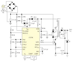
7-15. LT3798 flyback controller with single-stage active power-factor correction (PFC).
As shown in Fig. 7-15, the output transformer has three windings, including the output. The external MOSFET’s drain connects to one of the primary windings. The transformer’s third winding senses the output voltage and also supplies power for steady-state operation. The VIN pin supplies power to an internal LDO that generates 10V at the INTVCC pin. Internal control circuitry consists of two error amplifiers, minimum circuit, multiplier, transmission gate, current comparator, low output current oscillator, and master latch. Also, a sample-and-hold circuit monitors the third winding’s output voltage. A comparator detects the discontinuous conduction mode (DCM) with a capacitor and series resistor connected to the third winding.
During a typical cycle, the gate driver turns on the external MOSFET so that a current flows in the primary winding. This current increases at a rate proportional to the input voltage and inversely proportional to the transformer’s magnetizing inductance. The control loop determines the maximum current and a comparator turns off the switch when it reaches that current. When the switch turns off, the energy in the transformer flows out the secondary winding through the output diode, D1. This current decreases at a rate proportional to the output voltage. When the current decreases to zero, the output diode turns off and voltage across the secondary winding starts to oscillate from the parasitic capacitance and the magnetizing inductance of the transformer.
All windings have the same voltage across them, so the third winding rings, too. The capacitor connected to the DCM pin trips the comparator, which serves as a dv/dt detector, when ringing occurs. This timing information is used to calculate the output current. The dv/dt detector waits for the ringing waveform to reach its minimum value and then the switch turns on. This switching behavior is similar to zero volt switching and minimizes the amount of energy lost when the switch is turned on, improving efficiency as much as 5%. This IC operates on the edge of continuous and discontinuous conduction modes, which is called the critical conduction mode (or boundary conduction mode). Critical conduction mode operation enables use of a smaller transformer than continuous conduction mode designs.
SEPIC
The single-ended primary-inductance converter (SEPIC) is a dc/dc-converter topology that provides a positive regulated output voltage from an input voltage that varies from above to below the output voltage. The simplified SEPIC converter shown in Fig. 7-16 uses two inductors, L1 and L2, which can be wound on the same core because the same voltages are applied to them throughout the switching cycle. Using a coupled inductor takes up less space on the p.c. board and tends to be lower-cost than two separate inductors. The capacitor C4 isolates the input from the output and provides protection against a shorted load.
7-16. The two inductors in the basic SEPIC converter can be wound on the same core because the same voltages are applied to them throughout the switching cycle.
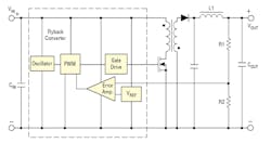
The IC regulates the output with current mode PWM control that turns on the power MOSFET Q1 at the beginning of each switching cycle. The input voltage is applied across the inductor and stores the energy as inductor current ramps up. During this portion of the switching cycle, the load current is provided by the output capacitor. When the inductor current rises to the threshold set by the error amplifier output, the power switch turns off and the external Schottky diode is forward biased. The inductor transfers stored energy to replenish the output capacitor and supply the load current. This operation repeats in every switching cycle. The duty cycle of the converter is determined by the PWM control comparator, which compares the error amplifier output and the current signal.
A ramp signal from the oscillator is added to the current ramp. This slope compensation is to avoid sub-harmonic oscillation that is intrinsic to the current mode control at duty cycle higher than 50%. The feedback loop regulates the FB pin to a reference voltage through an error amplifier. The output of the error amplifier is connected to the COMP pin. An external RC compensation network is connected to the COMP pin to optimize the feedback loop for stability and transient response.
TPS61170
The TPS61170 is a monolithic, high-voltage switching regulator from Texas instruments with an integrated 1.2A, 40V power MOSFET. The device can be configured in several standard regulator topologies, including boost and SEPIC. Figure 7-17 shows the SEPIC configuration. The device has a wide input-voltage range to support applications with input voltage from batteries or regulated 5V, 12V power rails.
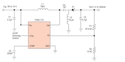
7-17. TPS61170 configured as a SEPIC converter.
The IC integrates a 40 V low-side FET for providing output voltages up to 38 V. The device regulates the output with current mode PWM (pulse width modulation) control. The switching frequency of the PWM is fixed at 1.2 MHz (typical). The PWM control circuitry turns on the switch at the beginning of each switching cycle. The input voltage is applied across the inductor and stores the energy as the inductor current ramps up. During this portion of the switching cycle, the load current is provided by the output capacitor. When the inductor current rises to the threshold set by the error amplifier output, the power switch turns off and the external Schottky diode is forward biased. The inductor transfers stored energy to replenish the output capacitor and supply the load current. This operation repeats each switching cycle. As shown in the block diagram, the duty cycle of the converter is determined by the PWM control comparator which compares the error amplifier output and the current signal.
The TPS61170 operates at a 1.2-MHz switching frequency, allowing the use of low-profile inductors and low-value ceramic input and output capacitors. It has built-in protection, including overcurrent limit, soft start and thermal shutdown.
Hysteretic Converter
The basic hysteretic regulator shown in Fig. 7-18 is a type of switching regulator that does not employ a PWM. It consists of a comparator with input hysteresis that compares the output feedback voltage with a reference voltage. When the feedback voltage exceeds the reference voltage, the comparator output goes low, turning off the buck-switch MOSFET. The switch remains off until the feedback voltage falls below the reference hysteresis voltage. Then, the comparator output goes high, turning on the switch and allowing the output voltage to rise again.
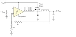
7-18. Basic hysteretic regulator represents the Fastest dc-dc converter control technique.
The basic hysteretic converter consists of an Error Comparator, control logic, and internal reference. The output usually drives a synchronous rectifier, which can be internal or external. A portion of the output voltage is fed back to the Error Comparator, which compares it with the reference voltage. If the output tends to go low relative to the reference voltage, the output capacitor charges up until it reaches equilibrium with the reference voltage. The comparator then turns on the synchronous rectifier. When the synchronous rectifier is on, the output voltage drops low enough to overcome the comparator’s hysteresis, at which time the synchronous rectifier turns off, starting a new cycle.
There is no voltage-error amplifier in the hysteretic regulator, so its response to any change in the load current or the input voltage is virtually instantaneous. Therefore, the hysteretic regulator represents the fastest possible dc-dc converter control technique. A disadvantage of the conventional hysteretic regulator is that its frequency varies proportionally with the output capacitor’s ESR. Since the initial value is often poorly controlled, and the ESR of electrolytic capacitors also changes with temperature and age, practical ESR variations can easily lead to frequency variations in the order of one to three. However, there is a modification of the hysteretic topology that eliminates the dependence of the operating frequency on the ESR.
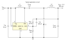
LM3475
The LM3475 is a buck (step-down) dc-dc controller that uses a hysteretic control architecture, which results in Pulse Frequency Modulated (PFM) regulation (Fig. 7-19). The hysteretic control scheme does not utilize an internal oscillator. Switching frequency depends on external components and operating conditions. Operating frequency decreases at light loads, resulting in excellent efficiency compared to PWM architectures. Because switching is directly controlled by the output conditions, hysteretic control provides exceptional load transient response.
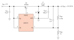
7-19. LM3475 is a buck (step-down) dc-dc controller that uses a hysteretic control architecture, which results in Pulse Frequency Modulated (PFM) regulation.
The LM3475 uses a comparator-based voltage control loop. The voltage on the feedback pin is compared to an 0.8V reference with 21mV of hysteresis. When the FB input to the comparator falls below the reference voltage, the output of the comparator goes low. This results in the driver output, PGATE, pulling the gate of the PFET low and turning on the PFET.
With the PFET on, the input supply charges COUT and supplies current to the load through the PFET and the inductor. Current through the inductor ramps up linearly, and the output voltage increases. As the FB voltage reaches the upper threshold (reference voltage plus hysteresis) the output of the comparator goes high, and the PGATE turns the PFET off. When the PFET turns off, the catch diode turns on, and the current through the inductor ramps down. As the output voltage falls below the reference voltage, the cycle repeats.
Cuk Converter
The Cuk converter is a dc-dc converter whose output voltage magnitude can be either greater than or less than the input voltage. It is essentially a boost converter followed by a buck converter with a capacitor to couple the energy. It is an inverting converter, so the output voltage is negative with respect to the input voltage. The non-isolated Cuk converter can only have opposite polarity between input and output. It uses a capacitor as its main energy-storage component, unlike most other types of converters that use an inductor.
As with other converters (buck converter, boost converter, buck-boost converter), the Cuk converter can either operate in continuous or discontinuous current mode. However, unlike these converters, it can also operate in discontinuous voltage mode (the voltage across the capacitor drops to zero during the commutation cycle).
The LM2611 from Texas Instruments is a Cuk converter that consists of a current mode controller with an integrated primary switch and integrated current sensing circuitry (Fig. 7-20). The feedback is connected to the internal error amplifier and it uses type II/III internal compensation. A ramp generator provides some slope compensation to the system. SHDN pin is a logic input designed to shut down the converter.
7-20. LM2611 configured as a Cuk converter
A current mode, fixed frequency PWM switching regulator the LM2611 has a −1.23V reference that makes it ideal for use in a Cuk converter. The Cuk converter inverts the input and can step up or step down the absolute value. Using inductors on both the input and output, the Cuk converter produces very little input and output current ripple. This is a significant advantage over other inverting topologies such as the buck-boost and flyback.
Multiphase Converter
As current requirements increase, so does the need for increasing the number of phases in the converter. Single-phase buck controllers are fine for low-voltage applications with currents of up to about 25 A, however power dissipation and efficiency are an issue at higher currents. One approach for higher current loads is the multiphase buck controller. Their performance makes them ideal for powering personal electronics, portable industrial, solid state drive, small-cell applications, FPGAs, and microprocessors.
The two-phase circuit shown in Fig. 7-21 has interleaved phases, which reduces ripple currents at the input and output. It also reduces hot spots on a printed circuit board or a particular component. A two-phase buck converter reduces RMS current power dissipation in the MOSFETs and inductors by half. Interleaving also reduces transitional losses.
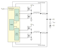
7-21. Basic multiphase converter has two phases that are interleaved, which reduces ripple currents at the input and output.
Multiphase cells operate at a common frequency, but are phase shifted so that conversion switching occurs at regular intervals controlled by a common control chip. The control chip staggers the switching time of each converter so that the phase angle between each converter switching is 360 deg./n, where n is the number of converter phases. The outputs of the converters are paralleled so that the effective output ripple frequency is n × f, where f is the operating frequency of each converter. This provides better dynamic performance and significantly less decoupling capacitance than a single-phase system.
Current sharing among the multiphase cells is necessary so that one does not hog too much current. Ideally, each multiphase cell should consume the same amount of current. To achieve equal current sharing, the output current for each cell must be monitored and controlled.
The multiphase approach also offers packaging advantages. Each converter delivers 1/n of the total output power, reducing the physical size and value of the magnetics employed in each phase. Also, the power semiconductors in each phase only need to handle 1/n of the total power. This spreads the internal power dissipation over multiple power devices, eliminating the concentrated heat sources and possibly the need for a heat sink. Even though this uses more components, its cost tradeoffs can be favorable.
Multiphase converters have important advantages:
- Reduced RMS current in the input filter capacitor, allows use of a smaller and less expensive types
- Distributed heat dissipation, reduces the hot-spot temperature, increasing reliability
- Higher total power capability
- Increased equivalent frequency without increased switching losses, which allows use of smaller equivalent inductances that shorten load transient time
- Reduced ripple current in the output capacitor reduces the output ripple voltage and allows use of smaller and less expensive output capacitors
- Excellent load transient response over the entire load range
Multiphase converters also have some disadvantages that should be considered when choosing the number of phases, such as:
• The need for more switches and output inductors than in a single-phase design, which leads to a higher system cost than a single-phase solution, at least below a certain power level
- More complex control
- The possibility of uneven current sharing among the phases
- Added circuit layout complexity
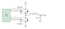
Synchronous Rectification
Efficiency is an important criterion in designing dc-dc converters, which means power losses must be minimized. These losses are cause by the power switch, magnetic elements, and the output rectifier. Reduction in power switch and magnetics losses require components that can operate efficiently at high switching frequencies. Output rectifiers can use Schottky diodes, but synchronous rectification (Fig. 7-22) consisting of power MOSFETS can provide higher efficiency.
7-23. Typical switch-mode power supply model with negative feedback employs a compensation block, G(s), and H(s), the open-loop gain. VIN(s) is the input and VOUT(s) is the output.
Also, to obtain a response converging toward a stable state we need to ensure that the phase where the loop gain magnitude is 1 is less than -180 deg. To make sure we stay away from the -180 deg. at the crossover frequency, the compensator G(s) must tailor the loop response at the selected crossover frequency to build the necessary phase margin. The appropriate phase margin ensures that despite external perturbations or unavoidable production spreads, changes in the loop gain will not put the system’s stability in jeopardy. The phase margin also impacts the transient response of the system. Therefore, the compensator, G(s) must provide the desired gain and phase characteristics.
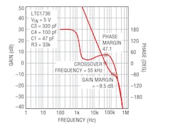
Using a network analyzer you can determine stability margins by measuring the gain and phase of the control loop, and then observe the resulting Bode plot (Fig. 7-24) that is a graph of the gain and phase versus frequency of a power supply. A 60-deg. phase margin is preferred, but 45 deg. is usually acceptable. A gain margin of –10dB is usually considered acceptable. Gain and phase margin are important because actual component values may vary over temperature. Thus, component values may differ from unit-to-unit in production, causing the control loop’s voltage gain and phase to vary accordingly. Plus, component values may vary over time, and cause instability.
7-25. The LM21305 is a switch-mode regulator IC that employs a single compensation node that requires compensation components RC and CC1 connected between the COMP pin and AGND.
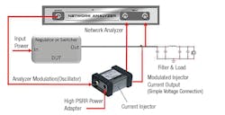
Determining the compensation for a power supply isn’t always easy because a Bode plot assessment is not feasible when there is no feedback loop access to the part. In other cases, the feedback loop is difficult to access because the hardware is integrated or would require cutting a PCB trace. In other cases, the devices either contain multiple control loops, with only one of them being accessible, or the order of the control loop is higher than second order, in which case the Bode plot is a poor predictor of relative stability. A further complication is that in many portable electronics, such as cell phones and tablets, the circuitry is very small and densely populated leaving little in the way of access to the control loop elements.
In the above cases the only way to verify stability is with non-invasive stability margin (NISM) assessment. It is derived from easily accessible output impedance measurements. The mathematical relationship that allows the precise determination of the control loop stability from output impedance data was developed by Picotest and incorporated into the OMICRON Lab Bode 100 Vector Network Analyzer (VNA) software. Figure 7-26 shows the test setup for this measurement.
7-27. CUI’s NDM2Z power-supply family employs auto compensation that allows it to dynamically set optimum stability and transient response.
The 50A NDM2Z supplies deliver 91% efficiency with 12 Vdc input and 1.0 Vdc output at 50% load. These supplies all have a 4.5 to14 Vdc input range and a programmable output of 0.6 to 5.0 Vdc in the 12A version and 0.6 to 3.3 Vdc in the 25A and 50A versions.
Module features include active current sharing, voltage sequencing, voltage tracking, synchronization and phase spreading, programmable soft start and stop, as well as a host of monitoring capabilities. CUI’s simple, easy-to-use GUI aids these designs.
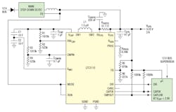
ZL8101
The NMD2Z uses an Intersil/Zilker ZL8101, voltage-mode, synchronous buck controller with a constant frequency pulse width modulator (PWM). This third-generation digital controller uses a dedicated, optimized, state machine for generating precise PWM pulses and a proprietary microcontroller used for setup, housekeeping, and optimization (Fig. 7-28). It requires external drivers, power MOSFETs, capacitors, and inductors. Integrated sub-regulation allows operation from a single 4.5V to 14V supply. Using simple pin connections or standard PMBus commands you can configure an extensive set of power management functions with Intersil’s PowerNavigator GUI.
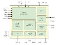
7-28. Intersil’s ZL8101 IC block diagram shows the PWM outputs (PWMH and PWML) that interface with an external driver like the ZL1505.
Initially, the ZL8101’s auto compensation measures the characteristics of the power train and determines the required compensation. The IC saves compensation values and uses them on subsequent inputs. Once enabled, the ZL8101 is ready to regulate power and perform power management tasks with no programming required. Advanced configuration options and real-time configuration changes are available via the I2C/SMBus interface. An on-chip non-volatile memory (NVM) saves configuration data.
You should choose the external power MOSFETs primarily on RDS(ON) and secondarily on total gate charge. The actual power converter’s output current depends on the characteristics of the drivers and output MOSFETs.
Configurable circuit protection features continuously safeguard the IC and load from damage due to system faults. The ZL8101 continuously monitors input voltage, output voltage/current, internal temperature, and temperature of an external thermal diode. You can also set monitoring parameters for specific fault condition alerts.
A non-linear response (NLR) loop improves the response time and reduces load transient output deviations. To optimize power converter efficiency, the ZL8101monitors its operating conditions and continuously adjusts the turn-on and turn-off timing of the high-side and low-side power MOSFETs. Adaptive performance optimization algorithms such as dead-time control, diode emulation, and adaptive frequency provide greater efficiency improvement.
A Power-Good (PG) signal indicates the output voltage is within a specified tolerance of its target level and no fault condition exists. By default, the PG pin asserts if the output is within -10%/+15% of the target voltage. You can change these limits and the polarity via the I2C/SMBus interface.
An internal phase-locked loop (PLL) serves as a clock for internal circuitry. You can drive the PLL from an external clock source connected to the SYNC pin. You can set the switching frequency from 200kHz to 1.33MHz.
A Windows-based GUI enables full configuration and monitoring capability via the I2C/SMBus interface.
CUI’s NDM3Z-90 is a 90A module that has several features that enable high power conversion efficiency. Adaptive algorithms and cycle-by-cycle charge management improves the response time and reduces the output deviation as a result of load transients.
ZL8800
The NDM3Z uses the Intersil ZL8800 for auto compensation. It is a dual output or dual phase digital dc/dc controller. Each output can operate independently or be used together in a dual phase configuration for high current applications. The ZL8800 supports a wide range of output voltages (0.54V to 5.5V) operating from input voltages as low as 4.5V up to 14V. Figure 7-29 shows the two-phase configuration that employs external DRMOS power modules.
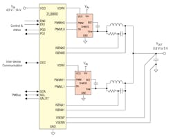
7-29. Intersil’s ZL8800 configured as a two-phase converter
With the fully digital ChargeMode Control, the ZL8800 will respond to a transient load step within a single switching cycle. This unique compensation-free modulation technique allows designs to meet transient specifications with minimum output capacitance thus saving cost and board space.
Intersil’s proprietary single wire DDC (Digital-DC) serial bus enables the ZL8800 to communicate between other Intersil ICs. By using the DDC, the ZL8800 achieves complex functions such as inter-IC phase current balancing, sequencing and fault spreading, eliminating complicated power supply managers with numerous external discrete components.
The ZL8800 features cycle-by-cycle output overcurrent protection. The input voltage, output voltages, and DrMOS/MOSFET driver supply voltages are under- and overvoltage protected. Two external and one internal temperature sensors are available for temperature monitoring, one of which is used for under and over-temperature protection. A snapshot parametric capture feature allows users to take a snapshot of operating and fault data during normal or fault conditions.
Integrated Low Dropout (LDO) regulators allow the ZL8800 to be operated from a single input supply eliminating the need for additional linear regulators. The LDO output can be used to power external drivers or DrMOS devices.
With full PMBus compliance, the ZL8800 is capable of measuring and reporting input voltage, input current, output voltage, output current as well as the device’s internal temperature, external temperatures and an auxiliary voltage input.
This supply incorporates a wide range of configurable power management features that are simple to implement with a minimum of external components. Additionally, the supply has protection features that continuously safeguard the load from damage due to unexpected system faults.
The supply’s standard configuration is suitable for a wide range of operation in terms of input voltage, output voltage, and load. The configuration is stored in an internal Non-Volatile Memory (NVM). All power-management functions can be reconfigured using the PMBus interface.
Powervation Auto Compensation
Bellnix Co. Ltd. (Japan) uses ROHM’s PV3012 Powervation digital controller in its low-profile, 60 A dc/dc module. The BDP12-0.6S60R0 digital power module is a PMBus compliant, non-isolated step-down converter that addresses the needs for small form-factor designs while providing high reliability and high performance. ROHM’s PV3012 is a digital two-phase controller (Fig. 7-30).
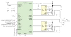
7-30. Powervation’s PV3012 IC is a real-time auto compensation IC with a single output, dual- or single-phase digital synchronous buck controller for POL applications.
The 60 A BDP uses, and parallel BDP module operation is supported via ROHM’s DSS current sharing bus. This PMBus compliant module features precision measurement and telemetry reporting, a full line of programmable power-supply protection features, power good, and optional tracking function, all in a compact 32.8 mm × 23.0 mm ROHS compliant SMD package design.
ROHM’s PV3012 Powervation digital controller is also used TDK-Lambda’s iJB Series high-current digital POL modules use. The iJB series products support low-voltage, high-current operation while providing ±0.5% set-point accuracy over line, load, and temperature range. While the PMBus functionality of the module provides real-time telemetry of voltage, current, and temperature and enables full programmability of the dc/dc converter, the iJB series products also employ function setting pins, enabling them to be used in non-PMBus applications.
Using the Powervation intelligent auto-tuning technology, Auto-Control, the iJB POL modules bring better dynamic performance and system stability to the application. Auto-Control is a patented adaptive compensation technology that optimizes dynamic performance and system stability in real-time without requiring any noise injection or the drawbacks of periodic techniques. This is a key benefit for modules and other designs that drive unknown or variable output loads, and addresses the challenges of load parameter drift that occurs over temperature and time.
Another PV3012 digital controller user is Murata Power Solutions’ the OKLF-T/25-W12N-C DC/DC module. It is a non-isolated, DC/DC converter delivering a maximum of 25 A at an output of 1.2 V, when operating up to 70°C with a 200 LFM airflow. The adjustable outputs provide precision regulation from 0.69 V to 3.63 V over a wide input range (6.5 V to 14 V).
Murata Power Solutions’ OKLF 25 A module delivers ultra-fast load transient response, exceptional de-rating performance, and >90% typical efficiency in a high power density form-factor. The module is a complete, stand-alone power supply; with the use of the PV3012 digital control IC, it provides a full-line of protection features and precision set-point accuracy.
This POL converter delivers precision set-point accuracy of ±0.5% over line, load, and temperature range – far better than analog options. Additionally, this offering adds value by the use of space saving elevated inductors and Powervation’s Auto-Control.
PV3204
One of the new Powervation products from ROHM that provide auto compensation is the PV3204, a dual phase digital synchronous buck controller with adaptive loop compensation, for point-of-load (POL) applications (Fig. 7-31). The output can supply 0.6 V to 5.5 V, and can be configured and controlled via PMBus or through programming stored in the non-volatile memory (NVM). Besides the SMBus interface, PV3204 provides a 3-bit parallel VID interface with a mapping from 0.85 V to 1.0 V in 25 mV steps, and 1.05 V.
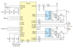
7-31. Powervation’s PV3204 is a dual-phase digital synchronous buck controller with adaptive loop auto-compensation, for point-of-load (POL) applications.
PV3204
PV3204 uses the Powervation proprietary adaptive digital control loop, Auto-Control, a real-time adaptive loop compensation technology for switching power converters that autonomously balances the trade-offs between dynamic performance and system stability. Auto-Control does away with complex calculations and setting optimum stability employed with traditional compensation techniques. Auto-Control adjusts P, I, and D coefficients each switching cycle to continuously achieve optimum stability over a wide range of disturbances. Auto-Control is embedded in the control architecture of the Powervation digital devices, and does not rely on injected noise of periodic calibrations. The continuous nature of Auto-Control allows it to manage changes in the system that occur in real-time, or slowly over time while the power supply is in use. This self-compensation occurs on a cycle-by-cycle basis, so Auto-Control is able to continuously adjust according to changes in temperature that occur while the power supply is in use, and accounts for other factors such as aging and drift.
This controller may be used in single- or dual-phase mode. When used in dual-phase mode, phases may be added or removed as the load varies, so that efficiency is maximized over the load range. Additionally, the outputs of the phases are interleaved so that the effective switching frequency at the output is doubled.
The digital functionality of this PMBus power converter controller allows system telemetry (remote measurement and reporting) of current, voltage, and temperature information.
Additionally, to maximize system performance and reliability, the IC provides temperature correction/compensation of several parameters.
Read more articles from the Power Management Series in the Power Management section of our Series Library.

About the Author

Sam Davis
Sam Davis was the editor-in-chief of Power Electronics Technology magazine and website that is now part of Electronic Design. He has 18 years experience in electronic engineering design and management, six years in public relations and 25 years as a trade press editor. He holds a BSEE from Case-Western Reserve University, and did graduate work at the same school and UCLA. Sam was the editor for PCIM, the predecessor to Power Electronics Technology, from 1984 to 2004. His engineering experience includes circuit and system design for Litton Systems, Bunker-Ramo, Rocketdyne, and Clevite Corporation.. Design tasks included analog circuits, display systems, power supplies, underwater ordnance systems, and test systems. He also served as a program manager for a Litton Systems Navy program.
Sam is the author of Computer Data Displays, a book published by Prentice-Hall in the U.S. and Japan in 1969. He is also a recipient of the Jesse Neal Award for trade press editorial excellence, and has one patent for naval ship construction that simplifies electronic system integration.
You can also check out his Power Electronics blog.
Comment About the Article
To join the conversation, and become an exclusive member of Electronic Design, create an account today!

Leaders relevant to this article: