Power Management Chapter 10: Silicon Power Management Power Semiconductors

This articles is part of the Power Management Series in the Power Management section of our Series Library.
Download this article as a .PDF eBook.
Silicon power semiconductors are employed in power management systems. They are found in two different forms:
• Discrete Power Semiconductors (single type
• Integrated Power Semiconductors
MOSFETs and BJTs (bipolar junction transistors) can be integrated with other circuits in a single package. In addition, various types of power semiconductors may housed in a hybrid (multi-chip module, or MCM) package, that is, interconnected with other monolithic discrete devices in the same package.
Power switches are actually the electronic equivalent of a mechanical switch, except for much faster switching speed. Fig. 10-1 is the representation of a mechanical switch. The individual power semiconductor switch applies power to a load when a control signal tells it to do so. The control signal also tells it to turn off. Ideally, the power semiconductor switch should turn on and off in zero time. It should have an infinite impedance when turned off so zero current flows to the load. It should also have zero impedance when turned on so that the on-state voltage drop is zero. Another idealistic characteristic would be that the switch input consumes zero power when the control signal is applied. However, these idealistic characteristics are unachievable with the present state of the art.
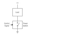
10-1. Power management power semiconductors duplicate the action of a mechanical switch in which a control operation turns the power semiconductor switch on and off to control power applied to a load.
In the real world, actual power semiconductor switches do not meet the ideal switching characteristics. For example, Fig. 10-2(a) shows a control signal applied to an ideal power semiconductor switch whose output exhibits zero transition time when turning on and off (Fig. 10-2(b)). When the transistor is off (not conducting current) power dissipation is very low because current is very low.
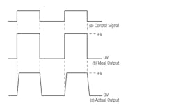
10-2. Actual power semiconductors do not meet the ideal switching characteristics.
(a) Control signal applied to an ideal power semiconductor switch whose
(b) Ideal output exhibits zero transition time when turning on and off.
(c) Actual power switch exhibits some delay when turning on and off.
When the transistor is on (conducting maximum current) power dissipation is low because the conducting resistance is low. In contrast, an actual power switch exhibits some delay when turning on and off, as shown in Fig. 10-2(c). Therefore, some power dissipation occurs when the switch goes through the linear region between on and off. This means that the most power dissipation depends on the time spent going from the off to on and vice versa, that is, going through the linear region. Thus, the faster the device goes through the linear region, the lower the power dissipation and losses.
Power MOSFETs
Power MOSFETS (Metal-Oxide Semiconductor Field Effect Transistors) are among the most widely used power switch semiconductors. Power MOSFETs are three-terminal silicon devices that function by applying a signal to the gate that controls current conduction between source and drain (Fig. 10-3). They are available in n-channel versions that require a positive gate turn-on voltage and also p-channel devices that require a negative gate voltage to turn on. Their current conduction capabilities are up to several tens of amperes, with breakdown voltage ratings (BVDSS) of 10V to 1000V.
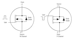
10-3. N-Channel and P-Channel Power MOSFETs showing the voltage polarity of the Drain and the gate pulse polarity to turn the device on.
MOSFETs used in integrated circuits are lateral devices with gate, source and drain all on the top of the device, with current flow taking place in a path parallel to the surface. The Vertical Double diffused MOSFET (VDMOS) uses the device substrate as the drain terminal. MOSFETs used in integrated circuits exhibit a higher on-resistance than those of discrete MOSFETs.
The fabrication processes used to manufacture power MOSFETs are the same as those used in today’s VLSI circuits, although the device geometry, voltage and current levels are significantly different. Discrete monolithic MOSFETs have tens or hundreds of thousands of individual cells paralleled together in order to reduce their on-resistance.
The gate turns the MOSFET on when its gate-to-source voltage is above a specific threshold. Typical gate thresholds range from 1 to 4 V. For an n-channel MOSFET a positive bias greater than the gate-to-source threshold voltage (VGS(th) ) is applied to the gate, a current flows between source and drain. For gate voltages less than VGS(th) the device remains in the off-state. P-channel MOSFETs use a negative gate drive signal to turn on.
When power semiconductor switches first found wide use, discrete transistors, pulse transformers, opto-couplers, among other components were used to drive the power MOSFET on and off. Now, specially designed gate driver ICs are used in many applications. This minimizes the drive requirements from a low power circuit, such as a microprocessor, and also acts as a buffer between the controlling signal and the power semiconductor switch. The gate driver supplies enough drive to ensure that the power switch turns on properly. Some gate drivers also have protection circuits to prevent failure of the power semiconductor switch and also its load.
MOSFET characteristics include several parameters critical to their performance:
Blocking voltage (BVDSS) is the maximum voltage that can be applied to the MOSFET. When driving an inductive load, this includes the applied voltage plus any inductively induced voltage. With inductive loads, the voltage across the MOSFET can actually be twice the applied voltage.
Maximum single pulse avalanche energy (EAS) determines how much energy the MOSFET can withstand under avalanche conditions. Avalanche occurs if the maximum drain-to-source voltage is exceeded and current rushes through the device. The higher the avalanche value the more rugged the device. The avalanche condition can cause two possible failure modes that can destroy a MOSFET. The most destructive is “bipolar latching” that occurs if the device current causes a voltage drop across its internal device resistance, resulting in transistor action and latching of the parasitic bipolar structure of the MOSFET. A second failure mode is thermal, which occurs if the avalanche condition raises the device temperature above its maximum junction temperature.
Trench technology offers an avalanche capability approaching industry-leading planar technology. To ensure satisfactory performance, devices in this technology can be fully characterized for single pulse avalanche energy (EAS) up to their maximum junction temperature. The higher the EAS, the more rugged the device. Some devices are rated in terms of EAR, the repetitive avalanche energy.
Trench technology provides the desirable characteristics of low on-resistance sometimes at the expense of high avalanche energy. Trench power MOSFET technology provides 15% lower device on-resistance per unit area than existing benchmark planar technologies but usually at the cost of higher charge. And, the trench technology allows 10% lower on-resistance temperature coefficient. Fig. 10-4 is plot of single pulse avalanche energy for a MOSFET.
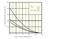
10-4. Avalanche occurs if the maximum drain-to-source voltage is exceeded and current rushes through the device.
On-resistance (RDS(ON)) for both planar and Trench MOSFETs is important because it determines the power loss and heating of the power semiconductor. The lower the on-resistance the lower the device power loss and the cooler it will operate. Low on-resistance drastically reduces heat-sinking requirements in many applications, which lowers parts count and assembly costs. In many applications, the low on-resistance also eliminates the need to parallel MOSFETs for low on-resistance, which leads to improved reliability and lower overall system cost than previous MOSFET generations. In virtually all MOSFETS, the n-channel versions have lower on-resistance than p-channel devices with the same operating voltages.
RDS(ON) decreases with increasing cell density. The cell density has increased over the years from around half a million per square inch in 1980 to around eight million for planar MOSFETs and around 12 million and higher for trench technology.
Maximum junction temperature, TJ(max), is a function of the electrical characteristics of the device itself, as well as the package employed. Package thermal properties determine its ability to extract heat from the die. The junction-to-ambient and junction-to-case thermal resistance is a measure of the MOSFET’s ability to extract heat. Data sheets rate thermal resistance in terms of either °C/W or K/W. The lower the thermal resistance, the more efficient the package is in eliminating heat. In some cases, a heat sink may be required to maintain the device junction temperature below its maximum rating. Fig. 10-5 shows the variation of RDS(ON) with junction temperature for VGS = 4.5 V and 10 V. VGS is gate-to-source voltage.
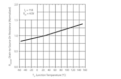
10-5. Normalized Variation of on-resistance vs. junction temperature for an N-Channel MOSFET.
Drain current (ID) establishes the ability of the MOSFET to drive a specific load. This value can be limited by the MOSFET’s package. When operated in the pulsed mode, the MOSFET’s drain current can be several times its continuous rating. In the pulsed mode the pulse width and duty cycle determine safe drain current and device power dissipation. Fig. 10-6 shows the maximum drain current vs. case temperature.
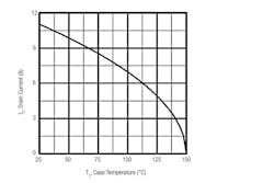
10-6. Maximum Drain Current for a typical N-Channel Power MOSFET.
Safe operating area (SOA) for a MOSFET is a function of the voltage and current applied to the device. Power semiconductor manufacturers include a curve in their power transistor data sheets (Fig. 10-7) that defines the allowable combination of voltage and current, which is called the device’s safe operating area (SOA). The product of the voltage and current represents the watts dissipated in the chip. If you exceed the SOA, the chip will get too hot and fail. MOSFET devices are limited by the SOA; bipolar devices have an additional failure mechanism called secondary breakdown that significantly reduces the SOA.
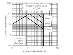
10-7. Typical Maximum Safe Operating for an N-Channel Power MOSFET
Total Gate charge (QG) The charge on the gate terminal of the MOSFET as determined by its gate-to-source capacitance. The lower the gate charge, the easier it is to drive the MOSFET. Total gate charge, QG, affects the highest reliable switching frequency of the MOSFET. The lower the gate charge, the higher the frequency. Operation at higher frequencies allows use of lower value, smaller size capacitors and inductors, which can be significant factors in system cost. A low gate charge also makes it easier to drive the MOSFET, however, designers sometimes need to trade-off switching frequency with EMI considerations. Some New trench devices exhibit lower gate charge than some existing planar technologies by replacing larger die with new smaller die devices that have been optimized to offer a lower charge version of the trench devices. Fig. 10-8 shows the gate charge for a typical power MOSFET, which is specified in nC, nano-coulombs.
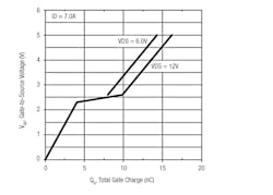
10-8. Total Gate Charge (Qg) of an N-Channel Power MOSFET Varies With the Drain-Source Voltage
Although input capacitance values are useful, they do not lend themselves to calculation of the gate current required to switch the device in a given time and they do not provide accurate results when comparing the switching performance of two devices. A more useful parameter from the circuit design point of view is the total gate charge. Most manufacturers include both parameters on their data sheets. Using gate charge, QG, the designer can calculate the amount of current required from the drive circuit to switch the device on in a desired length of time because QG = current × time. For example, a device with a gate charge of 20nC can be turned on in 20msec if a current of 1mA is supplied to the gate, or it can turn on in 20nsec if the gate current is increased to 1A. These simple calculations would not have been possible with input capacitance values.
Gate charge and on-resistance are inter-related. That is, the lower the gate charge, the higher the on-resistance and vice versa. Historically, MOSFET manufacturers have focused on reducing RDS(on) without paying much attention to gate charge. This has changed in the last several years, with new designs and processes becoming available that offer reduced gate charge devices.
Figure of Merit (FOM) relates to the tradeoff between RDS(ON) and gate charge. The product of RDS(ON) × QG is a figure of merit (FOM) that compares different power MOSFETs for use in high frequency applications.
Threshold Voltage (VGS(TH)) is the minimum gate-source electrode bias required to form a conducting channel between the source and the drain regions. It is usually measured at a drain-source current of 250μA. A value of 2-4V for high voltage devices with thicker gate oxides, and logic-compatible values of 1-2V for lower voltage devices with thinner gate oxides are common. In battery-based applications where power is a premium, the trend is towards lower values of RDS(on) and Vgsth. Gate oxide quality and integrity become major issues as gate oxide thickness is reduced to achieve lower Vgsth, the minimum voltage is required between the gate and source that enables the MOSFET to turn on. Logic level MOSFETs have typical values of about 2V to 3V, whereas other devices can have higher values. In Fig. 10-9 is the threshold voltage plotted against junction temperature.
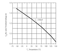
10-9. The Gate Threshold Voltage of this N-Channel Power MOSFET Is About 1.28 V for ID = 250μA at 25ºC.
Power Loss MOSFETs are expected to have low conduction and switching losses. For power management applications, conduction losses, ruggedness and avalanche capability are important features. Conduction losses are determined by the product of operating current and on-resistance (I2R) of the power MOSFET.
Maximum Allowable Power Dissipation (PD) is the maximum allowable power dissipation that raises the MOSFET’s die temperature to the maximum allowable junction temperature, Tjmax, when the case temperature is held at 25°C. Tj max is normally 150°C or 175°C.
Body-Diode Forward Voltage (VSD) is the guaranteed maximum forward drop of the body-drain diode at a specified value of source current. The value of VSD is significant and must be low in applications where the source-drain voltage may extend into the negative range, causing forward biasing the body-drain diode. If this happens, the source-drain current flows from drain straight to the source contacts, across the forward biased body-diode p-n junction.
A second and more dominant current conduction path will exist through the channel if the gate-source voltage, VGS >Vgsth. Low voltage and low RDS(on) power MOSFETs are used in such synchronous rectifier modes since their forward voltage drop can be as low as 0.1V versus the typical Schottky diode forward voltage drops of 0.4-0.5V. Maximum values of 1.6V for high voltage devices (>100V) and values of 1.2V for low voltage devices (<100V) are common for VSD. A typical source-drain diode forward voltage is shown in Fig. 10-10.
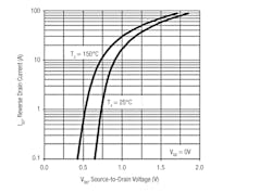
10-10. Body-Diode Forward Voltage for an N-Channel Power MOSFET.
Thermal Resistance, Junction-to-Case (RθJC) is the junction-to-case thermal impedance of the MOSFET, a typical surface mount package can have a thermal resistance of 30-50 °C/W, whereas a typical TO-220 device can be 2°C/W or less. Data sheets may also provide a value for RθJA for the junction-to-ambient thermal resistance of the power MOSFET
Maximum dV/dt is the maximum rate of rise of source-drain voltage allowed if the MOSFET’s dV/dt. If this rate is exceeded, the voltage across the gate-source terminals may become higher than the threshold voltage of the device, forcing the device into current conducting mode and under certain conditions a catastrophic failure may occur.
There are two possible mechanisms by which a dV/dt induced turn-on may take place. One becomes active through the feedback action of the gate-drain capacitance CGD together with CGS forming a capacitive divider that can generate a pulse sufficient to exceed the Vth and turn the device on during fast voltage transitions on the drain. When a voltage ramp appears across the drain and source terminals of the device. Usually the driver will sink a current flowing through the gate resistance, RG, to clamp the gate low during the off state, if Rg is too large, it is sometimes possible that the driver is isolated from the gate allowing the device to turn on. RG is the total gate resistance in the circuit.
The second mechanism for the dV/dt turn-on in MOSFETs is through the parasitic BJT. The capacitance associated with the depletion region of the body diode, extending into the drift region is denoted as CDB and appears between the base of the BJT and the drain of the MOSFET. This capacitance gives rise to a current that flows through the base resistance, RB, when a voltage ramp appears across the drain-source terminals.
Static Electricity (ESD) Effects is another way to kill semiconductors. The static charge accumulated by a person handling an MOSFET semiconductor is often enough to destroy the part. Therefore, manufacturers of semiconductors have instituted static discharge ratings that range from 3000V to 5000V. Handlers of MOSFET semiconductors use grounding straps and conductive surfaces to prevent static charge problems.
Switching and Transient Response is determined by the time required to establish voltage changes across capacitances and current changes in inductances. RG is the distributed resistance of the gate and is approximately inversely proportional to active area. Values of around 20 Ω-mm2 are common for the product of RG and active area for polysilicon gates. Fig. 10-11 shows the parasitics in the MOSFET input. Ls and LD are source and drain lead inductances and are around a few tens of nH. There are also several parasitic capacitances associated with the power MOSFET. Gate-source capacitance, CGS, is the capacitance due to the overlap of polysilicon gate with the source and the channel regions and is not a strong function of applied voltage. Fig. 10-12 illustrates the variation of the parasitic capacitances vs. the drain-source voltage.
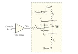
10-11. Typical N-Channel MOSFET’s Parasitic Capacitances Includes CGD (Gate-to-Drain), CDS (Drain-to-Source), and CGS (Gate-to-Source)
CRSS is the reverse transfer capacitance, which is the capacitance between the drain and gate with the source connected to ground. This capacitance is equal to the gate-to-drain capacitance. CRSS, often referred to as the Miller capacitance, is one of the major parameters affecting rise and fall times of the output voltage during switching. Plus, it also affects turn-off delay time. The capacitances decrease over a range of increasing drain-source voltage, especially the output and reverse transfer capacitances.
Important parameters for MOSFETs are listed in Table 10-1.

Power MOSFET Fabrication Technologies
The trench MOSFET has replaced the planar device in many applications because it extends the cell density limit. Trench technology allows a higher cell density but is more difficult to manufacture than the planar device. Process refinements have yielded devices with steadily increasing density and lower on-resistance. TrenchFET devices have achieved on-resistance less than 1mW for a 25mm2 silicon die, exclusive of lead resistance.
Trench MOSFETs employ the same schematic configuration of the older planar MOSFETs. And, new Trench MOSFETs offer significant advantages over the older generation Trench MOSFETs and also some improvements over the older planar MOSFET technology.
10-11. Typical N-Channel MOSFET’s Parasitic Capacitances Includes CGD (Gate-to-Drain), CDS (Drain-to-Source), and CGS (Gate-to-Source)
Among the other technologies are MDMesh . STMicroelectronics says that the improvement in RDS(ON) achieved with MDmesh V will significantly reduce losses in line-voltage PFC circuits and power supplies, which will in turn enable new generations of electronic products offering better energy ratings and smaller dimensions. This new technology should help designers with high efficiency targets and also save power.
MDmesh V achieves its RDS(ON) per area performance by improving the transistor drain structure to lower the drain-source voltage drop. This reduces the device’s on-state losses while also maintaining low gate charge (Qg), enabling energy-efficient switching at high speeds and delivering a low RDS(ON) x Qg Figure of Merit (FOM). ST claims that the breakdown voltage of 650V is also higher than competing 600V devices, delivering a valuable safety margin for designers. A further advantage of ST’s MDmesh V MOSFETs is a cleaner turn-off waveform, enabling easier gate control and simpler filtering due to reduced EMI.
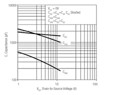
10-12. Typical Plot of N-Channel MOSFET’s Parasitic Capacitances vs. Drain-to-Source Voltage.
STMicroelectronics’ STripFET technology uses an optimized layout and updated manufacturing process to improve the gate charge, gate resistance and input capacitance characteristics. The low gate charge enables excellent switching behavior and the low gate resistance means fast transient response. The technology also offers an extremely low figure-of-merit, meaning reduced conduction and switching losses.
Among STMicroelectronics introductions is a series of 30V surface-mount power transistors, achieving on-resistance as low as 2 mΩ (max) to increase the energy efficiency of products such as computers, telecom and networking equipment. The latest-generation STripFET VI DeepGATE family process has high equivalent cell density and said to be best RDS(ON) in relation to active chip size. This is around 20 per cent better than the previous generation and allows the use of small surface-mount power packages in switching regulators and DC-to-DC converters, the company said.
Infineon has developed CoolMOS™ technology for high voltage Power MOSFETs that reduces the RDS(ON) area product by a factor of five for 600V transistors. It has redefined the dependence of RDS(ON) on the breakdown voltage. The more than square-law dependence in the case of a standard MOSFET has been broken and a linear voltage dependence achieved. It is said that this opens the way to new fields of application even without avalanche operation. System miniaturization, higher switching frequencies, lower circuit parasitics, higher efficiency, reduced system costs are pointing the way towards future developments. It has also set new benchmarks for device capacitances. Due to chip shrink and novel internal structure, the technology shows a very small input capacitance as well as a strongly nonlinear output capacitance. The drastically lower gate charge facilitates and reduces the cost of controllability, and the smaller feedback capacitance reduces dynamic losses. This technology, improves the minimum RDS(ON) values in the 600 to 1000 V operating range.
MOSFET Packages
MOSFETs are available in Small Outline IC (SOIC) packages for applications where space is at a premium. Larger through-hole TO-220, TO-247 and the surface mountable D2PAK or SMD-220 are also available. Newer package styles include chip scale devices and also the DirectFET™ and PolarPak™ packages.
Devices with breakdown voltage ratings of 55V-60V and gate-threshold voltages of 2 to 3V are used mainly in through-hole packages such as TO-220, TO-247 or the surface mounted D2PAK (SMD220). These through-hole packages have very low thermal resistance. Despite their higher thermal resistances, more surface-mount SOIC packages are finding their way into applications due to the continuous reduction in on-resistance of power MOSFETs. SOIC packages save space and simplify system assembly. The newest generation of power MOSFETs use chip scale and ball grid array packages for low voltage power MOSFETs.
The International Rectifier DirectFET power package is surface-mount power MOSFET packaging technology designed for efficient topside cooling in a SO-8 footprint (Fig. 10-13). In combination with improved bottom-side cooling, the new package can be cooled on both sides to cut part count by up to 60%, and board space by as much as 50% compared to devices in standard or enhanced SO-8 packages. This effectively doubles current density (A/in2) at a lower total system cost. The DirectFET MOSFET family offerings match 20V and 30V synchronous buck converter MOSFET chipsets, followed by the addition at 30V targeted for high frequency operation. The DirectFET MOSFET family is also available in three different can sizes.
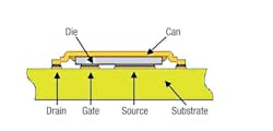
10-13. DirectFET® is a surface mount semiconductor for board-mounted power applications. It eliminates unnecessary elements of packaging that contribute to higher inductance and resistance, both thermal and electrical, so that its power capabilities exceed those of comparably sized packages.
Vishay’s PolarPAK® (Fig. 10-14) is a thermally enhanced package that facilitates MOSFET heat removal from an exposed top metal lead-frame connected to a drain surface in addition to a source lead-frame connected to a PCB. PolarPAK was specifically designed for easy handling and mounting onto the PCB with high-speed assembly equipment and thus to enable high assembly yields in mass-volume production. PolarPAK power MOSFETs have the same footprint dimensions of the standard SO-8, dissipate 1 °C/W from their top surface and 1 °C/W from their bottom surface. This provides a dual heat dissipation path that gives the devices twice the current density of the standard SO-8. With its improved junction-to-ambient thermal impedance, a PolarPAK power MOSFET can either handle more power or operate with a lower junction temperature. A lower junction temperature means a lower RDS(ON), which in turn means higher efficiency. A reduction in junction temperature of just 20 °C can also result in a 2.5 times increase in lifetime reliability.
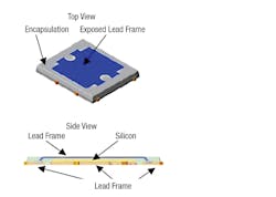
10-14. The PolarPAK™ package increases the power handling capability of power MOSFETs while keeping a PCB landing pattern no bigger in area than that of a standard SO-8 orPowerPAK® SO-8.
DrMOS
Intel’s November 2004 DrMOS specification identified a multi-chip module consisting of a gate driver and power MOSFET. A major advantage of using this module (Fig. 10-15) is that the individual MOSFET’s performance characteristics can be optimized, whereas monolithic MOSFETs produce higher on-resistance. Although the component cost of a multi-chip module may be higher than a monolithic part. The designer must view the cost from a system viewpoint.
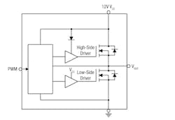
10-15. DrMOS Is a Multi-Chip Module That Contains Two MOSFETs and the Associated Drive Circuits.
That is, space is saved, potential noise problems are minimized, and fewer components reduce production time and cost. Here, the multi-chip approach is superior to use of a monolithic part.
Unlike discrete solutions whose parasitic elements combined with board layout significantly reduce system efficiency, the DrMOS module is designed to both thermally and electrically minimize parasitic effects and improve overall system efficiency. In operation, the high-side MOSFET is optimized for fast switching while the low-side device is optimized for low RDS(ON). This arrangement ideally accommodates the low-duty-cycle switching requirements needed to convert the 12V bus to supply the processor core with 1.0V to 1.2V at up to 40A.
SiC632CD
Vishay Intertechnology’s SiC632CD integrated DrMOS power stage for multiphase POL regulator applications combines power MOSFETs, advanced MOSFET gate driver IC, and a bootstrap Schottky diode (Fig. 10-16). Housed in thermally enhanced 5 mm by 5 mm PowerPAK MLP55-31L package, it offers a 45 % smaller footprint compared with discrete solutions. The devices are suitable for industrial PC and high-current multiphase modules used in networking and industrial applications.
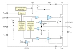
10-16. Vishay Intertechnology’s SiC632CD integrated DrMOS power stage for multiphase POL regulator applications combines power MOSFETs, advanced MOSFET gate driver IC, and a bootstrap Schottky diode.
This integrated device offers continuous current up to 40 A in the 5 mm by 5 mm PowerPAK MLP55-31L package. Besides its high-current capabilities and footprint savings, the power stage also lowers package parasitics to enable switching frequencies up to 2 MHz — further shrinking the overall solution size and profile by reducing the size of the output filter. Its high- and low-side MOSFETs utilize Gen IV TrenchFET® technology to reduce switching and conduction losses. The integrated power driver IC is compatible with a wide range of PWM controllers and supports tri-state PWM logic of 5 V.
The SiC632CD is optimized for synchronous buck converters, DC/DC voltage regulation modules, and multiphase VRDs for CPUs, GPUs, and memory. To increase light-load efficiency in these applications, the driver IC incorporates diode emulation mode circuitry and zero-current detect. An adaptive dead time control helps to further improve efficiency at all load points. To support PS4 mode light-load requirements for IMVP8, the power stages reduce current consumption to 5 µA when systems are operating in standby mode, and they can awake from this state within 5 µs. Protection features for the RoHS-compliant, halogen-free devices include undervoltage lockout (UVLO).
Power MOSFETs for Synchronous Rectifiers
Fig. 10-17 shows a simplified synchronous rectifier circuit. Typical synchronous rectifiers consist of high-side and low-side MOSFETs, which require different characteristics for an optimum design. Generally, the best high side MOSFET is one with the lowest Qswitch × RDS(ON) figure-of-merit. Qswitch is defined as the post gate threshold portion of the gate-to-source charge plus the gate-to-drain charge (Qgs2 + Qgd). In contrast, the best high side MOSFET must exhibit very low RDS(ON) coupled with good Cdv/dt immunity.
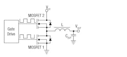
10-17. A Synchronous Rectifier Employs Two N-Channel MOSFETs, Which Provides More Efficient Rectification than Conventional Diodes.
Power MOSFETs for Automotive Applications
Over the last two decades Power MOSFETs have evolved as a necessary power handling component is virtually all automobiles. To be eligible for use in automotive electronic systems these power MOSFETs must meet the AEC Q101 standard. Some new power MOSFETs are AEC Q101 qualified and will fit in the growing use of electric motors, solenoids and fuel injectors. Power MOSFETs have low on-resistance, 40 V and 100 V maximum operating voltage and the ability to tolerate the high-voltage transients such as load dump that can occur in automotive electrical systems.
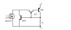
10-18 Simplified IGBT equivalent circuit
An important feature of these new MOSFETs is their Moisture Sensitivity Level, or MSL. This relates to the packaging and handling precautions for semiconductors and is an electronic standard for the time the device can be exposed to ambient room conditions of approximately 30°C/60%RH. The reason this is important is that thin fine-pitch devices could be damaged during surface mount technology (SMT) reflow when moisture trapped inside the component expands. Trapped moisture can damage a semiconductor. In extreme cases, cracks will extend to the component surface.
According to IPC/JEDEC’s J-STD-20: Moisture/Reflow Sensitivity Classification for Plastic Integrated Circuit (IC) SMTs, there are eight levels of moisture sensitivity. Originally MOSFETs was rated at MSL 3, which allowed 168 hours of moisture testing. MSL 1 allows an unlimited time for the moisture test.
Today, there are new applications and power MOSFETs continue to grab them. . This includes Electric Power Steering (EPS) and Micro Hybrid Vehicles, and chassis, drive train and power train systems. Besides meeting the AEC Q101 standard, they must meet the cost constraints imposed by automotive manufacturers.
For EPS, an electric motor driven by a power MOSFET provides steering assist to the driver of a vehicle. A typical system employs sensors detect the motion and torque of the steering column, and a computer module controls system performance. Software allows varying amounts of assistance to be applied depending on driving conditions.
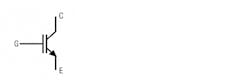
10-19. IGBT circuit symbol
Electric systems have a fuel efficiency advantage over conventional hydraulic power steering. The electrical approach eliminates the belt-driven hydraulic pump constantly running, whether assistance is required or not. Another major advantage is the elimination of a belt-driven engine accessory, and several high-pressure hydraulic hoses between the hydraulic pump, mounted on the engine, and the steering gear, mounted on the chassis. This simplifies manufacturing and maintenance.
A micro-hybrid system performs a stop-start function completely transparent to the driver, during idling, like waiting for a traffic light, a starter-alternator turns off the engine. Then, the engine restarts very quickly and silently when the drive steps on the accelerator. This technique cuts fuel consumption and gas emissions at standstill. Tests have shown that this can cut fuel consumption about 6%.
Power MOSFETs have played a major role make automotive systems more reliable. Among the traditional mechanical components that have been eliminated are shafts, pumps, hoses, fluids, coolers, etc., which reduces the weight of the vehicle and improves fuel efficiency. Safety improvement is another feature of electronic controls that provide more automated functions that cannot be achieved by mechanical techniques. Compared with mechanical systems, the electronics trend also allows easier modification or upgrade of automotive systems.
MSL-1 preconditioning is required for surface mount capable devices that are put on Temperature Cycling, H3TRB, IOL, and Autoclave tests. If straight leaded devices (such as I-PAK or TO-262) are used, then the devices are required to undergo the preconditioning with a third reflow exposure in lieu of the surface mounting step
MOSFETs and BJT Comparison
Power MOSFETs are capable of operating at very high frequencies compared with Bipolar Junction Transistors (BJTs) whose switching speed is much slower than for a power MOSFET of similar size and voltage rating. Typical rise and fall times of power MOSFETs are of the order of several nanoseconds which is two orders of magnitude faster than bipolar devices of similar voltage rating and active area. BJTs are limited to frequencies of less than 100kHz whereas power MOSFETs can operate up to 1MHz before switching losses become unacceptably high. Recent advances in the design and processing of MOSFETs are pushing this frequency limit higher.
Power MOSFETs are voltage controlled devices with simple drive circuitry requirements. Power BJTs on the other hand are current controlled devices requiring large base drive currents to keep the device in the ON state. Power MOSFETs have been replacing power BJTs in power application due to faster switching capability and ease of drive, despite the very advanced state of manufacturability and lower costs of BJTs.
BJTs suffer from thermal runaway. The forward voltage drop of a BJT decreases with increasing temperature potentially leading to destruction. This is of special significance when several devices are paralleled in order to reduce forward voltage drop. Power MOSFETs can be paralleled easily because the forward voltage increases with temperature, ensuring an even distribution of current among all components. They can withstand simultaneous application of high current and high voltage without undergoing destructive failure due to second breakdown. However, at high breakdown voltages (>~200V) the on-state voltage drop of the power MOSFET becomes higher than that of a similar size bipolar device with similar voltage rating, making it more attractive to use the bipolar power transistor at the expense of worse high-frequency performance.
Breakdown voltage (BVDSS) is the drain-to-source voltage at which a current of 250μA starts to flow between source and drain while the gate and the source are shorted together. With no bias on the gate, the drain voltage is entirely supported by the reverse-biased body-drain p-n junction. Breakdown voltage is primarily determined by the resistivity of the epitaxial layer.
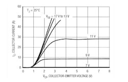
10-20. Output characteristics of the 15A, 600V NGTB15N60EG at 25°C
All applications of power MOSFET switches require some guardbanding when specifying BVDSS rating. It is important to remember that there is a price to be paid for this in the form of either higher RDS(on) or larger die. There may be applications where a reduction of conservative guardbanding on BVDSS can be justified by an improved RDS(on) specification or lower cost without jeopardizing performance or reliability.
Bipolar transistors have ratings for maximum current under continuous and pulsed conditions. Exceeding these ratings usually result in device failure. Current ratings on MOSFET transistors have a different meaning because they behave as a resistor when they turn on. This means that the maximum voltage drop or heat generated determines the maximum current. Turning the current on and off at high speeds reduces the average power or heat generated, thereby increasing the maximum allowable current.
Power semiconductor Reliability
Excessive operating voltage can cause power semiconductor failures because the devices may have small spacing between their internal elements. An even worse condition for a power semiconductor is to have high voltage and high current present simultaneously. A few nanoseconds at an excessive voltage or excessive current can cause a failure. Most power semiconductor data sheets specify the maximum voltage that can be applied under all conditions. The military has shown very clearly that operating semiconductors at 20% below their voltage rating provides a substantial improvement in their reliability.
Another common killer of power semiconductors is heat. Not only does high temperature destroy devices, but even operation at elevated, non-destructive temperatures can degrade useful life. Data sheets specify a maximum junction temperature, which is typically between 100°C and 200oC for silicon. Most power transistors have a maximum junction rating of 125°C to 150°C, the safe operating temperature is much lower.
Transient Effects
Power semiconductors can be destroyed by very short pulses of energy. A major source of destructive transients is caused by turning on or off an inductive load. Protection against these problems involves a careful combination of operating voltage and current margins and protective devices.
Power dv/dt and di/dt
The terms dv/dt and di/dt reflect a time rate of change of voltage (dv/dt) or current (di/dt) describe their reaction to turning on or off a reactive load. These problems can occur in power semiconductor switches because all sections of the device do not behave in an identical manner when subjected to very high rates of change. It is not only important to look at the dv/dt and di/dt values generated within a circuit, but also turn on and turn off times as well.
EMI
Switching power on and off at a rapid rate can cause electromagnetic interference (EMI) that can affect nearby electronic systems. Domestic and international standards define the amount of EMI that can be emitted.
Unclamped Inductive Switching (UIS)
Whenever current through an inductance is turned off quickly, the resulting magnetic field induces a counter electromagnetic force (CEMF) that can build up surprisingly high potentials across the switch. With transistor switches, the full buildup of this induced potential may far exceed the rated voltage breakdown of the transistor, resulting in catastrophic failure.
There are two failure modes when subjecting a MOSFET to UIS. These failure mechanisms are considered as either active or passive. The active mode results when the avalanche current forces the MOSFET’s parasitic bipolar transistor into conduction. In the passive mode the instantaneous device temperature reaches a critical value. At this elevated temperature the MOSFET’s parasitic bipolar transistor causes catastrophic thermal runaway. In both cases the MOSFET is destroyed.
Cost Considerations
As a semiconductor chip gets larger its cost grows exponentially. And, there is the cost of the package that houses the integrated power device and the cost of interconnections. In deciding whether to integrate a power semiconductor into an integrated circuit or use two separate devices, look at the die size of each. If an integrated power semiconductor and a discrete power semiconductor have large die, the die cost dominates the overall cost, it would be cheaper to use two parts.
Integrated power semiconductors make sense when the die sizes are moderate, or there are multiple outputs. This is so because the package and handling costs offset the increased silicon cost. A major impact on cost is the number of good devices that can be obtained from silicon wafer, usually called yield. Not only does a larger die size mean a disproportionately larger cost, but key parameters may not be the same for all functions of each device on the die.
IGBT
An insulated-gate bipolar transistor (IGBT) is a three-terminal power semiconductor device primarily used as an electronic switch that combines high efficiency and relatively fast switching. The IGBT provides the simple gate-drive characteristics of MOSFETs with the high-current and low-saturation-voltage capability of bipolar transistors. It combines an isolated-gate FET for the control input and a bipolar power transistor as a switch in a single device.
The IGBT is used in medium- to high-power applications like switch-mode power supplies, traction motor control and induction heating. Large IGBT modules typically consist of many devices in parallel and can have very high current-handling capabilities in the order of hundreds of amperes with blocking voltages of 6000 V. These IGBTs can control loads of hundreds of kilowatts. It is equally suitable in resonant-mode converter circuits.
The main advantages of IGBT over a Power MOSFET and a BJT are:
- Low on-state voltage drop due to conductivity modulation and on-state current density. So smaller chip size is possible, reducing cost.
- Low driving power and a simple drive circuit due to the input MOS gate structure, which allows relatively easy control compared with current controlled devices in high voltage and high current applications.
- Compared with a bipolar transistor, it has better current conduction capability as well as forward and reverse blocking capabilities.
Main disadvantages are:
- Slower switching speed compared with a power MOSFET, but better than a BJT.
- Possibility of latchup due to the internal PNPN thyristor structure.
A simple equivalent circuit model of an IGBT is shown in Fig. 10-18. It contains MOSFET, JFET, NPN and PNP transistors. The collector of the PNP is connected to the base of the NPN and the collector of the NPN is connected to the base of the PNP through the JFET. The NPN and PNP transistors represent the parasitic thyristor that constitutes a regenerative feedback loop. The resistor RB represents the shorting of the base-emitter of the NPN transistor to ensure that the thyristor does not latch up, which will lead to the IGBT latchup. The JFET represents the constriction of current between any two neighboring IGBT cells. It supports most of the voltage and allows the MOSFET to be a low voltage type and consequently have a low RDS(ON) value. A circuit symbol for the IGBT is shown in Fig. 10-19. It has three terminals called Collector (C), Gate (G) and Emitter (E).
In general, high voltage, high current and low switching frequencies favor the IGBT while low voltage, low current and high switching frequencies are the domain of the MOSFET.
There two types of IGBTs: Non-punch-through (NPT) and punch-through (PT). The PT type has an extra buffer layer that performs two functions:
- Avoids failure by punch-through action because the depletion region expansion at applied high voltage is restricted by this layer.
- Reduces the tail current during turn-off and shortens the fall time of the IGBT.
NPT IGBTs have equal forward and reverse breakdown voltage, so they are suitable for ac applications. PT IGBTs have less reverse breakdown voltage than the forward breakdown voltage, so they are applicable for dc circuits where devices are not required to support voltage in the reverse direction.
The IGBT has a much lower “on-state” resistance, RON than an equivalent MOSFET. This means that the I2R drop across the bipolar output structure for a given switching current is much lower. The forward blocking operation of the IGBT transistor is identical to a power MOSFET.
When used as static controlled switch, the IGBT has voltage and current ratings similar to that of the bipolar transistor. However, the presence of an isolated gate in an IGBT makes it a lot simpler to drive than the BJT as it requires much less drive power.
An IGBT is turned “ON” or “OFF” by activating and deactivating its Gate terminal. Applying a positive input voltage signal across the Gate and the Emitter will keep the device in its “ON” state, while making the input gate signal zero or slightly negative will cause it to turn “OFF” in much the same way as a bipolar transistor or MOSFET. Another advantage of the IGBT is that it has a much lower on-state channel resistance than a standard MOSFET.
The IGBT is a voltage-controlled device, so it only requires a small voltage on the gate to maintain conduction through the device unlike BJT’s that require that the Base current is continuously supplied in a sufficient enough quantity to maintain saturation.
Also, it is a unidirectional device, meaning it can only switch current in the “forward direction”, that is from collector to emitter unlike MOSFET’s that have bi-directional current switching capabilities (controlled in the forward direction and uncontrolled in the reverse direction).
The principal of operation and gate drive circuits for the IGBT are similar to that of the N-channel power MOSFET. The basic difference is that the resistance offered by the main conducting channel when current flows through the device in its “ON” state is very much smaller in the IGBT. Because of this, the current ratings are much higher than an equivalent power MOSFET.
The main advantages of using the IGBT over other types of transistors are its high voltage capability, low ON-resistance, ease of drive, relatively fast switching speeds and combined with zero gate drive current makes it a good choice for moderate speed, high voltage applications such as in pulse-width modulated (PWM), variable speed control, switch-mode power supplies or solar powered DC-AC inverter and frequency converter applications operating in the hundreds of kilohertz range.
One of the main advantages of the IGBT transistor is the simplicity by which it can be driven “ON” by applying a positive gate voltage, or switched “OFF” by making the gate signal zero or slightly negative allowing it to be used in a variety of switching applications.
With its lower on-state resistance and conduction losses as well as its ability to switch high voltages at high frequencies without damage makes the IGBT ideal for driving inductive loads such as coil windings, electromagnets and dc motors.
ON Semiconductor’s (now onsemi) NGTB15N60EG IGBT features a robust and cost effective Non−Punch Through (NPT) Trench construction. It is intended for switching applications and offers both low on state voltage and minimal switching loss. Therefore the IGBT is well suited for motor drive control and other hard switching applications. Incorporated into the device is a rugged co−packaged reverse recovery diode with a low forward voltage. Figure 10-20 is this IGBT’s output characteristics at 25°C.
Features
- Low Saturation Voltage Resulting in Low Conduction Loss
- Low Switching Loss in Higher Frequency Applications
- Soft Fast Reverse Recovery Diode
- 10 _s Short Circuit Capability
- Excellent Current versus Package Size Performance Density
- This is a Pb−Free Device
Read more articles from the Power Management Series in the Power Management section of our Series Library.
About the Author

Sam Davis
Sam Davis was the editor-in-chief of Power Electronics Technology magazine and website that is now part of Electronic Design. He has 18 years experience in electronic engineering design and management, six years in public relations and 25 years as a trade press editor. He holds a BSEE from Case-Western Reserve University, and did graduate work at the same school and UCLA. Sam was the editor for PCIM, the predecessor to Power Electronics Technology, from 1984 to 2004. His engineering experience includes circuit and system design for Litton Systems, Bunker-Ramo, Rocketdyne, and Clevite Corporation.. Design tasks included analog circuits, display systems, power supplies, underwater ordnance systems, and test systems. He also served as a program manager for a Litton Systems Navy program.
Sam is the author of Computer Data Displays, a book published by Prentice-Hall in the U.S. and Japan in 1969. He is also a recipient of the Jesse Neal Award for trade press editorial excellence, and has one patent for naval ship construction that simplifies electronic system integration.
You can also check out his Power Electronics blog.
Comment About the Article
To join the conversation, and become an exclusive member of Electronic Design, create an account today!

Leaders relevant to this article: