Power Management Chapter 13: Energy Harvesting

This articles is part of the Power Management Series in the Power Management section of our Series Library.
Download this article as a .PDF eBook.
Energy harvesting is the process by which ambient energy is captured and converted into electricity for small autonomous devices, such as satellites, laptops and nodes in sensor networks without the need for battery power. Energy harvesting applications reach from vehicles to the smart grid.
With electronic circuits now capable of operating at microwatt levels, it is feasible to power them from non-traditional sources. This has led to energy harvesting, which provides the power to charge, supplement or replace batteries in systems where battery use is inconvenient, impractical, expensive or dangerous. It can also eliminate the need for wires to carry power or to transmit data. Energy harvesting can power smart wireless sensor networks to monitor and optimize complex industrial processes, remote field installations and building HVAC. In addition, otherwise wasted energy from industrial processes, solar panels, or internal combustion engines, can be harvested for useful purposes. A key component in energy harvesting is a power converter that can operate with ultralow voltage inputs.
Now that we have described why it is feasible and what it can do, how does energy harvesting actually work? Put simply, it is a process that:
- Captures minute amounts of energy
- Accumulates that energy
- Stores the energy
- Maintains the stored energy as a power source
Typical energy harvesting inputs include:
- Solar power
- Thermal energy
- Wind energy
- Salinity gradients
- Kinetic energy
Today, energy harvesters do not usually produce enough energy to perform mechanical work, however they provide small amounts of power to support low-energy electronics. In most cases, the “fuel” ” for energy harvesters is naturally present and may be considered free. Using natural sources in remote areas for energy harvesting is an attractive alternative to inconvenient utility and battery power. These natural energy sources may be available maintenance-free for a lifetime. Energy harvesting can also be an alternative energy source that supplements the primary power source and enhances its reliability.
Energy harvesters are intended for applications requiring very low average power, but require periodic pulses of higher load current. For example, in many wireless sensor applications the circuitry is only powered to make measurements and transmit data periodically at a low duty cycle.
Energy harvesting is becoming more feasible today because of the increased efficiency of devices capable of capturing, storing, and producing electrical energy. This can be accomplished with the help of very efficient, very low-voltage input step-up converters. Also, improved low-voltage, high-efficiency microprocessors may allow them to become participants in energy harvesting systems.
Energy Harvesting IC
Linear Technology’s LTC3108, a highly integrated dc-dc converter is intended for energy harvesting. It can harvest and manage surplus energy from extremely low-input voltage sources such as TEG (thermoelectric generators), thermopiles. and small solar cells.
The circuit in Fig. 13-1 uses a small step-up transformer to boost the input voltage to an LTC3108 that provides a complete power-management solution for wireless sensing and data acquisition. It can harvest small temperature differences and generate system power instead of using traditional battery power. The LTC3108 is available in a small, thermally enhanced12-lead (4mm × 3mm) DFN and a 16-lead SSOP packages.
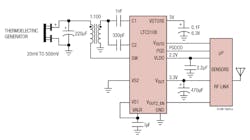
13-1. LTC3108 provides power management for wireless sensing and data acquisition
The LTC3108 utilizes a MOSFET switch to form a resonant step-up oscillator using an external step-up transformer and a small coupling capacitor. This allows it to boost input voltages as low as 20mV, high enough to provide multiple regulated output voltages for powering other circuits. The frequency of oscillation is determined by the inductance of the transformer secondary winding and is typically in the range of 20kHz to 200kHz. For input voltages as low as 20mV, a primary-secondary turns ratio of about 1:100 is recommended. For higher input voltages, this ratio can be lower.
The ac voltage produced on the secondary winding of the transformer is boosted and rectified using an external-charge pump capacitor (from the secondary winding to pin C1) and the rectifiers internal to the LTC3108. The rectifier circuit feeds current into the VAUX pin, providing charge to the external VAUX capacitor and the other outputs.
LDO Output
A 2.2V LDO can support a low-power processor or other low-power ICs. The LDO is powered by the higher value of either VAUX or VOUT. This enables it to become active as soon as VAUX has charged to 2.3V, while the VOUT storage capacitor is still charging. In the event of a step load on the LDO output, current can come from the main VOUT capacitor if VAUX drops below VOUT. The LDO requires a 1μF ceramic capacitor for stability. Larger capacitor values can be used without limitation, but will increase the time it takes for all the outputs to charge up. The LDO output is current limited to 4mA typical.
For pulsed-load applications, size the VOUT capacitor to provide the necessary current for a pulse on load. The capacitor’s value will be dictated by the load current, duration of the load pulse, and the voltage droop the circuit can tolerate. The capacitor must be rated for whatever voltage has been selected for VOUT by VS1 and VS2 (Table 13-1).
There must be enough energy available from the input voltage source for VOUT to recharge the capacitor during the interval between load pulses. Reducing the duty cycle of the load pulse allows operation with less input energy. The VSTORE capacitor may be a very large value (thousands of microfarads or even Farads) to provide holdup at times when the input power may be lost. Note that this capacitor can charge all the way to 5.25V (regardless of the settings for VOUT), so ensure that the holdup capacitor has a working voltage rating of at least 5.5V at the temperature for which it will be used. Fig. 13-2 plots the time for voltage to build up to its final value for a given input voltage and the input transformer turns ratio. The LTC3108’s extremely low quiescent current (<6µA) and high-efficiency design ensure the fastest possible charge times for the output reservoir capacitor.
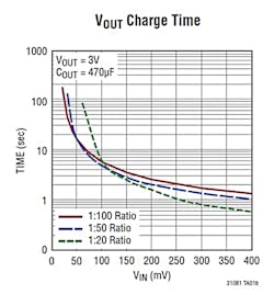
13-2. Plot of time for voltage to build up to its final value using the LTC3108.
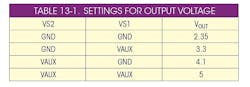
As listed in Table 13-1 above, the main output is pin-selectable via VS1 and VS2 for one of four fixed voltages (2.35V, 3.3V, 4.1V, or 5V) to power a wireless transmitter or sensors. A second switched output can be enabled by the host to power devices that do not have a micropower shutdown capability. The addition of a storage capacitor provides continuous power even when the input energy source is unavailable.
A power-good comparator monitors VOUT. The PGD pin is an open-drain output with a weak pull-up (1MΩ) to the LDO voltage. Once VOUT charges to within 7% of its regulated voltage, the PGOOD output goes high. If VOUT drops more than 9% from its regulated voltage, PGD goes low. The PGD output is designed to drive a microprocessor or other chip I/O and is not intended to drive a higher current load such as an LED. Pulling PGOOD up externally to a voltage greater than VLDO will cause a small current to be sourced into VLDO. PGOOD can be pulled low in a wire-OR configuration with other circuitry.
VOUT2 is an output that can be turned on and off by the host, using the VOUT2_EN pin. When enabled, VOUT2 is connected to VOUT through a 1.3Ω P-channel MOSFET switch. This output, controlled by a host processor, can be used to power external circuits such as sensors and amplifiers, that do not have a low power sleep or shutdown capability. VOUT2 can be used to power these circuits only when they are needed.
Piezoelectric Energy Harvesting
Linear Technology’s LTC3588-1 is an ultralow quiescent current power supply for energy harvesting and/or low current step-down applications (Fig. 13-3). The IC interfaces directly to a piezoelectric or alternative ac power source, to rectify a voltage waveform and store harvested energy on an external capacitor, bleed off any excess power via an internal shunt regulator, and maintain a regulated output voltage by means of a nanopower high-efficiency synchronous buck regulator.
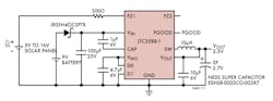
13-3. The LTC3588-1 employs a high efficiency buck converter to harvest solar energy and then convert it to a well-regulated output.
The LTC3588-1 has an internal full-wave bridge rectifier accessible via the differential PZ1 and PZ2 inputs that rectifies ac inputs such as those from a piezoelectric element. The rectified output is stored on a capacitor at the VIN pin and can be used as an energy reservoir for the buck converter. The low-loss bridge rectifier has a total drop of about 400mV with typical piezo generated currents (~10μA). The bridge is capable of carrying up to 50mA. One side of the bridge can be operated as a single-ended DC input. PZ1 and PZ2 should never be shorted together when the bridge is in use.
When the voltage on VIN rises above the UVLO rising threshold the buck converter is enabled and charge is transferred from the input capacitor to the output capacitor. A wide (~1V) UVLO hysteresis window is employed with a lower threshold approximately 300mV above the selected regulated output voltage to prevent short cycling during buck power-up. When the input capacitor voltage is depleted below the UVLO falling threshold, the buck converter is disabled. Extremely low quiescent current (450nA typical) in UVLO allows energy to accumulate on the input capacitor in situations where energy must be harvested from low power sources.
You can configure the LTC3588-1 for use with dc sources such as a solar panel as shown in Fig. 13-3 by connecting them to one of the PZ1/PZ2 inputs. Connecting the source in this way prevents reverse current from flowing in each element. Current limiting resistors should be used to protect the PZ1 or PZ2 pins. This can be combined with a battery backup connected to VIN with a blocking diode.
Analog Devices’ ADP5091/92 is an intelligent integrated energy harvesting nano-powered management solution that converts dc power from PV cells or thermoelectric generators (Fig. 13-4).The IC charges storage elements such as rechargeable Li-Ion batteries, thin film batteries, super capacitors, or conventional capacitors, and powers up small electronic devices and battery-free systems.
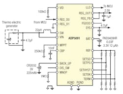
13-4. The ADP5091/92 provides efficient conversion of the harvested limited power from a 16 μW to 600 mW range with sub-μW operation losses.
The ADP5091/92 provides efficient conversion of the harvested limited power from a 16 μW to 600 mW range with sub-μW operation losses. With the internal cold-start circuit, the regulator can start operating at an input voltage as low as 380 mV. After a cold startup, the regulator is functional at an input voltage range of 80 mV to 3.3 V. You can program an additional 150mA regulated output with an external resistor divider or VID pin.
By sensing the input voltage, the control loop keeps the input voltage ripple in a fixed range to maintain stable dc-to-dc boost conversion. The OCV dynamic sensing mode and none-sensing mode both programming regulation points of the input voltage allow extraction of the highest possible energy from the harvester. A programmable minimum operation threshold (MINOP) enables boost shutdown during a low light condition. As a low light indicator for microprocessor, the LLD is the MIONP comparator output. In addition, the DIS_SW pin can temporarily shut down the boost regulator and is RF transmission friendly.
The charging control function of ADP5091/92 protects rechargeable energy storage, which is achieved by monitoring the battery voltage with programmable charging termination voltage and shutdown discharging voltage. In addition, a programmable PGOOD flag with programmable hysteresis monitors the SYS voltage.
An optional primary cell battery can be connected and managed by an integrated power path management control block that is programmable to switch the power source from the energy harvester, rechargeable battery, and primary cell battery.
The ADP5091/92 is available in a 24-lead LFCSP and is rated for a −40°C to +125°C junction temperature range.
Read more articles from the Power Management Series in the Power Management section of our Series Library.

About the Author

Sam Davis
Sam Davis was the editor-in-chief of Power Electronics Technology magazine and website that is now part of Electronic Design. He has 18 years experience in electronic engineering design and management, six years in public relations and 25 years as a trade press editor. He holds a BSEE from Case-Western Reserve University, and did graduate work at the same school and UCLA. Sam was the editor for PCIM, the predecessor to Power Electronics Technology, from 1984 to 2004. His engineering experience includes circuit and system design for Litton Systems, Bunker-Ramo, Rocketdyne, and Clevite Corporation.. Design tasks included analog circuits, display systems, power supplies, underwater ordnance systems, and test systems. He also served as a program manager for a Litton Systems Navy program.
Sam is the author of Computer Data Displays, a book published by Prentice-Hall in the U.S. and Japan in 1969. He is also a recipient of the Jesse Neal Award for trade press editorial excellence, and has one patent for naval ship construction that simplifies electronic system integration.
You can also check out his Power Electronics blog.
Comment About the Article
To join the conversation, and become an exclusive member of Electronic Design, create an account today!

Leaders relevant to this article: