Power Management Chapter 15: Photovoltaic Systems

This articles is part of the Power Management Series in the Power Management section of our Series Library.
Download this article as a .PDF eBook.
A photovoltaic cell converts light energy directly into electricity by the photovoltaic effect, which is a physical and chemical phenomenon. It is defined as a device whose electrical characteristics, such as current, voltage, or resistance, vary when exposed to light. Solar cells are the building blocks of photovoltaic modules, known as solar panels.
Multiple solar cells in an integrated group, all oriented in one plane, constitute a solar photovoltaic panel or solar photovoltaic module. Photovoltaic modules often have a sheet of glass on the sun-facing side, allowing light to pass while protecting the semiconductor wafers. Solar cells are usually connected in series in modules, creating an additive voltage. Connecting cells in parallel yields a higher current; however, problems such as shadow effects can shut down the weaker (less illuminated) parallel string (a number of series-connected cells) causing substantial power loss and possible damage because of the reverse bias applied to the shadowed cells by their illuminated partners. Strings of series cells are usually handled independently and not connected in parallel, though (as of 2014) individual power boxes are often supplied for each module, and are connected in parallel. Although modules can be interconnected to create an array with the desired peak dc voltage and loading current capacity, using independent MPPTs (maximum power point trackers) is preferable. Otherwise, shunt diodes can reduce shadowing power loss in arrays with series/parallel connected cells.
Adjusting for inflation, it cost $96 per watt for a solar module in the mid-1970s. Process improvements and a very large boost in production have brought that figure down 99%, to 68 cents per watt in 2016, according to data from Bloomberg New Energy Finance. Swanson’s Law is an observation similar to Moore’s Law that states that solar cell prices fall 20% for every doubling of industry capacity.
During the 1990s, polysilicon (“poly”) cells became increasingly popular. These cells offer less efficiency than their mono-silicon (“mono”) counterparts, but they are grown in large vats that reduce cost. By the mid-2000s, poly was dominant in the low-cost panel market, but more recently the mono returned to widespread use.
Manufacturers of wafer-based cells responded to high silicon prices in 2004-08 with rapid reductions in silicon consumption. Current cells use 8-9 grams (0.28-0.32 oz) of silicon per watt of power generation, with wafer thicknesses in the neighborhood of 200 microns.
The overall efficiency is the product of these individual metrics, which are:
• Charge carrier separation efficiency
• Reflectance efficiency
• Thermodynamic efficiency
• Conductive efficiency
A solar cell has a voltage-dependent efficiency curve, temperature coefficients, and allowable shadow angles.
Due to the difficulty in measuring these parameters directly, other parameters are substituted:
• Thermodynamic efficiency
• Quantum efficiency
• Integrated quantum efficiency
• VOC ratio
• Fill factor
Reflectance losses are a portion of quantum efficiency under “external quantum efficiency.” Recombination losses make up another portion of quantum efficiency, VOC ratio, and fill factor. Resistive losses are predominantly categorized under fill factor, but also make up minor portions of quantum efficiency, VOC ratio, ”OC” is open circuit.
The Fill Factor is the ratio of the actual maximum obtainable power to the product of the open circuit voltage and short circuit current. This is a key parameter in evaluating performance. In 2009, typical commercial solar cells had a Fill Factor > 0.70. Grade B cells were usually between 0.4 to 0.7. Cells with a high Fill Factor have a low equivalent series resistance and a high equivalent shunt resistance, so less of the current produced by the cell is dissipated in internal losses.
Single p–n junction crystalline silicon devices are now approaching the theoretical limiting power efficiency of 33.7%, noted as the Shockley–Queisser limit in 1961. In the extreme, with an infinite number of layers, the corresponding limit is 86% using concentrated sunlight.
For triple-junction thin-film solar cells, the world record is 13.6%, set in June 2015.
Solar cells can be classified into first-, second-, and third-generation cells.
• First-generation cells—also called conventional, traditional, or wafer-based cells—are made of crystalline silicon, the commercially predominant PV technology that includes materials such as polysilicon and monocrystalline silicon.
• Second-generation cells are thin-film solar cells that include amorphous silicon, CdTe, and CIGS cells and are commercially significant in utility-scale photovoltaic power stations, building integrated photovoltaics or in small stand-alone power system.
• Third-generation solar cells include a number of thin-film technologies often described as emerging photovoltaics—most of them have not yet been commercially applied and are still in the research or development phase. Many use organic materials, often organometallic compounds as well as inorganic substances. Despite the fact that their efficiencies had been low and the stability of the absorber material was often too short for commercial applications, there is a lot of research invested into these technologies as they promise to achieve the goal of producing low-cost, high-efficiency solar cells.
By far, the most prevalent bulk material for solar cells is crystalline silicon (c-Si), also known as “solar grade silicon.” Bulk silicon is separated into multiple categories according to crystallinity and crystal size in the resulting ingot, ribbon, or wafer. These cells are entirely based around the concept of a p-n junction. Solar cells made of c-Si are made from wafers between 160 to 240 micrometers thick.
Monocrystalline silicon (mono-Si) solar cells are more efficient and more expensive than most other types of cells. The corners of the cells look clipped, like an octagon, because the wafer material is cut from cylindrical ingots that are typically grown by the Czochralski process. Solar panels using mono-Si cells display a distinctive pattern of small white diamonds.
Epitaxial wafers can be grown on a monocrystalline silicon “seed” wafer by atmospheric-pressure CVD in a high-throughput inline process, and then detached as self-supporting wafers of some standard thickness (e.g., 250 µm) that can be manipulated by hand, and directly substituted for wafer cells cut from monocrystalline silicon ingots. Solar cells made with this technique can have efficiencies approaching those of wafer-cut cells, but at appreciably lower cost.
Polycrystalline silicon, or multi-crystalline silicon (multi-Si) cells are made from cast square ingots—large blocks of molten silicon carefully cooled and solidified. They consist of small crystals giving the material its typical metal flake effect. Polysilicon cells are the most common type used in photovoltaics and are less expensive, but also less efficient, than those made from monocrystalline silicon.
Ribbon silicon is a type of polycrystalline silicon—it is formed by drawing flat thin films from molten silicon and results in a polycrystalline structure. These cells are cheaper to make than multi-Si, due to a great reduction in silicon waste, as this approach does not require sawing from ingots. However, they are also less efficient.
Thin-film solar-cell technologies reduce the amount of active material in a cell. Most designs sandwich active material between two panes of glass. Since silicon solar panels only use one pane of glass, thin film panels are approximately twice as heavy as crystalline silicon panels, although they have a smaller ecological impact (determined from life-cycle analysis). The majority of film panels have 2-3 percentage points lower conversion efficiencies than crystalline silicon. Cadmium telluride (CdTe), copper indium gallium selenide (CIGS), and amorphous silicon (a-Si) are three thin-film technologies often used for outdoor applications. Thin-film solar cells are increasing due to it being silent, renewable, and solar energy being the most abundant energy source on Earth.
Cadmium telluride is the only thin-film material so far to rival crystalline silicon in cost/watt. However, cadmium is highly toxic and tellurium (anion: “telluride”) supplies are limited. The cadmium present in the cells would be toxic if released. However, release is impossible during normal operation of the cells and is unlikely during fires in residential roofs. A square meter of CdTe contains approximately the same amount of Cd as a single C cell nickel-cadmium battery, in a more stable and less soluble form.
Copper indium gallium selenide (CIGS) is a direct band gap material. It has the highest efficiency (~20%) among all commercially significant thin film materials. Traditional methods of fabrication involve vacuum processes including co-evaporation and sputtering. Recent developments attempt to lower the cost by using non-vacuum solution processes.
Silicon thin-film cells are mainly deposited by chemical vapor deposition (typically plasma-enhanced, PE-CVD) from silane gas and hydrogen gas. Depending on the deposition parameters, this can yield amorphous silicon (a-Si or a-Si:H), protocrystalline silicon, or nanocrystalline silicon (nc-Si or nc-Si:H), also called microcrystalline silicon.
Amorphous silicon is the most well-developed thin film technology to-date. An amorphous silicon (a-Si) solar cell is made of non-crystalline or microcrystalline silicon. Amorphous silicon has a higher bandgap (1.7 eV) than crystalline silicon (c-Si) (1.1 eV), which means it absorbs the visible part of the solar spectrum more strongly than the higher-power density infrared portion of the spectrum. The production of a-Si thin-film solar cells uses glass as a substrate and deposits a very thin layer of silicon by plasma-enhanced chemical vapor deposition (PECVD).
Protocrystalline silicon with a low-volume fraction of nanocrystalline silicon is optimal for high open-circuit voltage. Nc-Si has about the same bandgap as c-Si and nc-Si and a-Si can advantageously be combined in thin layers, creating a layered cell called a tandem cell. The top cell in a-Si absorbs the visible light and leaves the infrared part of the spectrum for the bottom cell in nc-Si.
Gallium arsenide (GaAs) is also used for single-crystalline thin film solar cells. Although GaAs cells are very expensive, they hold the world’s record in efficiency for a single-junction solar cell at 28.8%. GaAs is more commonly used in multi-junction photovoltaic cells for concentrated photovoltaics (CPV, HCPV) and for solar panels on spacecrafts, as the industry favors efficiency over cost for space-based solar power.
PV cells come in many sizes and shapes, from smaller than a postage stamp to several inches across. They are often connected together to form PV modules that may be up to several feet long and a few feet wide.
Modules, in turn, can be combined and connected to form PV arrays of different sizes and power output. The modules of the array make up the major part of a PV system, which can also include electrical connections, mounting hardware, power-conditioning equipment, and batteries that store solar energy for use when the sun is not shining.
PV Arrays are made up of PV modules, which are environmentally sealed collections of PV Cells. The most common PV module is 5 to 25 square feet in size and weighing about 3 to 4 lb/sq. ft. Often sets of four or more smaller modules are framed or attached together by struts in what is called a panel. This panel is typically around 19 to 35 square feet in area for ease of handling on a roof. This allows some assembly and wiring functions to be done on the ground if called for by the installation instructions.
When light shines on a PV cell, it may be reflected, absorbed, or pass right through. But only the absorbed light generates electricity. The energy of the absorbed light is transferred to electrons in the atoms of the PV cell semiconductor material. With their newfound energy, these electrons escape from their normal positions in the atoms and become part of the electrical flow, or current, in an electrical circuit. A special electrical property of the PV cell—what is called a “built-in electric field”—provides the force, or voltage, needed to drive the current through an external load, such as a light bulb.
Solar Modules
The heart of a photovoltaic system is the solar module. Many photovoltaic cells are wired together by the manufacturer to produce a solar module. When installed at a site, solar modules are wired together in series to form strings. Strings of modules are connected in parallel to form an array.
Module Types–Rigid flat-framed modules are currently most common and most of these are composed of silicon. Silicon cells have atomic structures that are single-crystalline (mono-crystalline), poly-crystalline (multi-crystalline), or amorphous (thin film silicon). Other cell materials used in solar modules are cadmium telluride (CdTe, commonly pronounced “CadTel”) and copper indium diselenide (CIS). Some modules are manufactured using combinations of these materials. An example is a thin film of amorphous silicon deposited onto a substrate of single-crystalline silicon.
In 2005, approximately 90% of modules sold in the United States were composed of crystalline silicon, either single-crystalline or poly-crystalline. The market share of crystalline silicon is down from previous years, however, and continues to drop as sales of amorphous silicon, CdTe and CIS modules are growing.
Rated Power–Grid-connected residential PV systems use modules with rated power output ranging from 100 to 300 watts. Modules as small as 10 watts are used for other applications. Rated power is the maximum power the panel can produce with 1,000 watts of sunlight per square meter at a module temperature of 25°C or 77°F in still air. Actual conditions will rarely match rated conditions and so actual power output will almost always be less.
PV System Voltage–Modern systems without batteries are typically wired to provide from 235V to 600V. In battery-based systems, the trend is also toward use of higher array voltages, although many charge controllers still require lower voltages of 12V, 24V, or 48V to match the voltage of the battery string.
Using Manufacturer’s Product Information to Compare Modules–Since module costs and efficiencies continue to change as technology and manufacturing methods improve, it is difficult to provide general recommendations that will be true into the future regarding, for example, which type of module is cheapest or the best overall choice. It is best to make comparisons based on current information provided by manufacturers, combined with the specific requirements of your application.
Two figures that are useful in comparing modules are:
• Price per watt
• Rated power output per area (or efficiency)
When looking through a manufacturer’s catalog of solar modules, you will often find the rated power, the overall dimensions of the module, and its price. Find the cost per watt by dividing the module’s price by its rated output in watts. Find the watts per area, by dividing its rated output by its area.
Module Cost per Watt–As a general rule, thin film modules have lower costs than crystalline silicon modules for modules of similar powers.
Module Efficiency (Watts per Area)–Modules with higher efficiency will have a higher ratio of watts to area. The higher the efficiency, the smaller the area (i.e., fewer modules) will be required to achieve the same power output of an array. Installation and racking costs will be less with more efficient modules, but this must be weighed against the higher cost of the modules. Amorphous silicon, thin-film CdTe, and CIS modules have rated efficiencies that are lower than crystalline silicon modules, but improvements in efficiency continue.
Arrays are most commonly mounted on roofs or on steel poles set in concrete. In certain applications, they may be mounted at ground level or on building walls. Solar modules can also be mounted to serve as part or all of a shade structure such as a patio cover. On roof-mounted systems, the PV array is typically mounted on fixed racks, parallel to the roof for aesthetic reasons and stood off several inches above the roof surface to allow airflow that will keep them as cool as practical.
Adjustability–The tilt of sloped rooftop arrays is usually not changed, since this is inconvenient in many cases and sometimes dangerous. However, many mounting racks are adjustable, allowing resetting of the angle of the PV modules seasonally.
Tracking–Pole-mounted PV arrays can incorporate tracking devices that allow the array to automatically follow the sun. Tracked PV arrays can increase the system’s daily energy output by 25% to 40%. Despite the increased power output, tracking systems usually are not justified by the increased cost and complexity of the system.
Photovoltaic system types can be broadly classified by answers to the following questions:
• Will it be connected to the utility’s transmission grid?
• Will it produce alternating current (ac) or direct current (dc) electricity, or both?
• Will it have battery backup?
• Will it have backup by a diesel, gasoline, or propane generator set?
Grid-connected, or grid-intertied systems, generate approximately the same quality of alternating current (ac) electricity as is provided by your utility. The energy generated by a grid-connected system is used first to power the ac electrical needs of the home or business. Any surplus power that is generated is fed or “pushed” onto the electric utility’s transmission grid. Any of the building’s power requirements that are not met by the PV system are powered by the transmission grid. In this way, the grid can be thought of as a virtual battery bank for the building.
Common System Types–Most new PV systems being installed in the United States are grid-connected residential systems without battery backup. Many grid-connected ac systems are also being installed in commercial or public facilities.
There are two main types of grid-connected systems, although others exist:
• Grid-connected ac system with no battery or generator backup
• Grid-connected ac system with battery backup
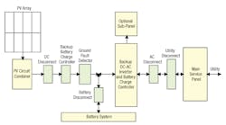
Example configurations of systems with and without batteries are shown in Fig. 15-1 and Fig. 15-2. Note there are common variations on the configurations shown, although the essential functions and general arrangement are similar.
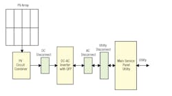
15-1. Grid-interactive with no battery backup only operates when the utility is available.
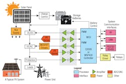
15-3. Solar inverters use maximum power point tracking (MPPT) to get the maximum possible power from the PV array.
The fill factor (FF) is a parameter which, in conjunction with the open-circuit voltage (VOC) and short circuit current(ISC) of the panel, determines the maximum power from a solar cell. Fill factor is defined as the ratio of the maximum power from the solar cell to the product of VOC and ISC.
ADSP-CM41x
Analog Devices’ ADSP-CM41x power-conversion platform employs a series of mixed-signal control processors intended to simplify system design, lower cost, and improve efficiency and safety in solar, energy storage, and electric vehicle infrastructure (Fig. 15-4). Solar panels and battery systems have a need for inverter technologies to drive the next wave of efficiencies in solar energy. Although disruptive new inverter designs are making improvements in size, weight, and cost reductions, they require further advances in digital processing to unlock their full potential. The ADSP-CM41x control processors represent a breakthrough in power conversion design, with an unmatched level of hardware integration specifically tailored to solar and other emerging energy applications. By alleviating the need for complex external circuitry, the ADSP-CM41x control processors deliver design time and cost reductions, safety improvements, and the precision gains intended to maximize the impact of new inverter designs.
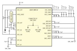
15-4. ADSP-CM41x (Analog Devices) power conversion platform employs a series of mixed-signal control processors intended to simplify system design, lower cost, and improve efficiency and safety in solar, energy storage, and electric vehicle infrastructure.
Central to the ADSP-CM41x design is its breakthrough “dual independent core” safety concept, which enables the integration of safety redundancy and functions into a single chip. This first-ever architecture saves considerable development time and system cost by eliminating the need for an external supervisory element, which is the current standard. Equally important is the on-board integration of optimized hardware accelerators, designed to offload work from the processor core and boost the processing power available for core functions. Additionally, the device’s on-board arc fault detection simplifies design, and enhances safety by using intelligent decision making to improve reliability and accuracy.
Building upon an already state-of-the-art power-conversion platform, the ADSP-CM41x establishes a new benchmark in ARM core processing and analog precision, adding to the industry performance established by the ADSP-CM40x power conversion series. The ADSP-CM41x series seamlessly integrates with other critical signal-chain components, including the AD740x sigma delta-based A/D converter, which replaces larger, more expensive sensor modules to reduce system cost and improve isolated current measurement. Also included in the platform is the ADuM413x series of isolated gate drivers featuring iCoupler isolation technology that enables faster switching to further increase system efficiency.
The ADSP-CM41xF family of mixed-signal control processors is based on the ARM Cortex-M4TM processor core with floating point unit operating at frequencies up to 240 MHz, and the ARM Cortex-M0TM processor core operating at frequencies up to 100 MHz. The processors integrate up to 160K Bytes of SRAM memory with ECC, up to 1M Byte of flash memory with ECC, accelerators and peripherals optimized for motor control and photovoltaic inverter control, and an analog module consisting of up to two 16-bit SAR-type ADCs, one 14-bit ADC and one 12-bit DAC. The ADSP-CM41xF family operates from a single voltage supply, generating its own internal voltage supplies using internal voltage regulators and an external pass transistor.
By integrating a rich set of industry-leading system peripherals and memory, the ADSP-CM41xF mixed-signal control processors are the platform of choice for next-generation applications that require RISC programmability and leading-edge signal processing in one integrated package.
Micro-Inverter
A micro-inverter converts dc from a single solar module to ac. The output from several micro-inverters is combined and often fed to the electrical grid. Micro-inverters contrast with conventional string and central solar inverters, which are connected to multiple solar modules or panels of the PV system.
Micro-inverters’ main advantage is that small amounts of shading, debris, or snow lines on any one solar module, or even a complete module failure, do not disproportionately reduce the output of the entire array. Each micro-inverter harvests optimum power by performing maximum power-point tracking for its connected module. Simplicity in system design, simplified stock management, and added safety are other factors introduced with the micro-inverter solution.
The primary disadvantages of a micro-inverter include a higher initial equipment cost per peak watt than the equivalent power of a central inverter, and increased installation time since each inverter needs to be installed adjacent to a panel (usually on a roof). This also makes them harder to maintain and more costly to remove and replace (O&M). Some manufacturers have addressed these issues with panels with built-in micro-inverters.
The main problem with the “string inverter” approach is the string of panels acts as if it were a single larger panel with a max current rating equivalent to the poorest performer in the string. For example, if one panel in a string has 5% higher resistance due to a minor manufacturing defect, the entire string suffers a 5% performance loss. This situation is dynamic. If a panel is shaded its output drops dramatically, affecting the output of the string, even if the other panels are not shaded. Even slight changes in orientation can cause output loss in this fashion. However, this effect is not entirely accurate and ignores the complex interaction between modern string inverter maximum power point tracking and even module bypass diodes.
Efficiency of a panel’s output is strongly affected by the load the inverter places on it. To maximize production, inverters use a technique called maximum power point tracking (MPPT) to ensure optimal energy harvest by adjusting the applied load. However, the same issues that cause output to vary from panel to panel affect the proper load that the MPPT system should apply. If a single panel operates at a different point, a string inverter can only see the overall change, and moves the MPPT point to match. This results in not just losses from the shadowed panel, but the other panels, too. Shading of as little as 9% of the surface of an array can, in some circumstances, reduce systemwide power as much as 54%. However, as stated above, these yearly yield losses are relatively small and newer technologies allow some string inverters to significantly reduce the effects of partial shading.
Other challenges associated with centralized inverters include the space required to locate the device, as well as heat dissipation requirements. Large central inverters are typically actively cooled. Cooling fans make noise, so location of the inverter relative to offices and occupied areas must be considered. And because cooling fans have moving parts, dirt, dust, and moisture can negatively affect their performance over time. String inverters are quieter but might produce a humming noise in late afternoon when inverter power is low.
Grid-Tie Inverter
A grid-tie inverter is a power inverter that converts dc into ac with an ability to synchronize its interface with a utility line. Its applications are converting dc sources such as solar panels or small wind turbines into ac for tying with the grid. Fig. 15-5 shows a diagram of a grid-tie inverter installation.
15-5. Conventional power converter architecture includes a solar inverter, which accepts the low dc output voltage from a photovoltaic array and produces an ac line voltage.
The grid-tie inverter (GTI) must synchronize its frequency with that of the grid (50 or 60 Hz) using a local oscillator and limit the voltage to no higher than the grid voltage. A high-quality modern GTI has a fixed-unity power factor, which means its output voltage and current are perfectly lined up, and its phase angle is within 1 deg. of the ac power grid. The inverter has an on-board computer that senses the current AC grid waveform, and outputs a voltage to correspond with the grid. However, supplying reactive power to the grid might be necessary to keep the voltage in the local grid inside allowed limitations. Otherwise, in a grid segment with considerable power from renewable sources, voltage levels might rise too much at times of high production.
Grid-tie inverters must quickly disconnect from the grid if the utility grid goes down. This is an NEC requirement that ensures that in the event of a blackout, the grid tie inverter will shut down to prevent the energy it transfers from harming any line workers who are sent to fix the power grid.
Technologies available to grid-tie inverters include newer high-frequency transformers, conventional low-frequency transformers, or they may operate without transformers altogether. Instead of converting direct current directly to 120 or 240 volts ac, high-frequency transformers employ a computerized multi-step process that involves converting the power to high-frequency ac and then back to dc and then to the final ac output voltage.
Most grid-tie inverters include a maximum power point tracker on the input side that enables the inverter to extract a maximum amount of power from its intended power source. Since MPPT algorithms differ for solar panels and wind turbines, specially made inverters for each of these power sources are available.
A charge controller may be used to power dc equipment with solar panels. The charge controller provides a regulated dc output and stores excess energy in a battery as well as monitoring the battery voltage to prevent under/overcharging. More expensive units also perform maximum power point tracking.
Inverter manufacturer datasheets generally include the following information:
• Rated output power in watts or kilowatts: some inverters may provide an output rating for different output voltages.
• Output voltage(s): indicates to which utility voltages the inverter can connect and may also produce three phase power.
• Peak efficiency: represents the highest efficiency that the inverter can achieve.
• CEC weighted efficiency: this efficiency is published by the California Energy Commission on its GoSolar website. This is an average efficiency and is a better representation of the inverter’s operating profile.
• Maximum input current: maximum dc the inverter can use.
• Maximum output current: The maximum continuous ac that the inverter will supply.
• Peak power tracking voltage: dc voltage range in which the inverter’s maximum point power tracker will operate.
• Start voltage: indicates the minimum dc voltage that is required in order for the inverter to turn on and begin operation.
• IPxx rating: the Ingress Protection rating or IP Code classifies and rates the level of protection provided against the ingress of solid foreign objects (first digit) or water (second digit), a higher digit means greater protection. In the United States, the NEMA enclosure type is used similarly to the international rating.
Balance of system equipment (BOS) includes mounting systems and wiring systems used to integrate the solar modules into the structural and electrical systems of the home. The wiring systems include disconnects for the dc and ac sides of the inverter, ground-fault protection, and overcurrent protection for the solar modules. Most systems include a combiner board of some kind since most modules require fusing for each module source circuit. Some inverters include this fusing and combining function within the inverter enclosure.
Read more articles from the Power Management Series in the Power Management section of our Series Library.

About the Author

Sam Davis
Sam Davis was the editor-in-chief of Power Electronics Technology magazine and website that is now part of Electronic Design. He has 18 years experience in electronic engineering design and management, six years in public relations and 25 years as a trade press editor. He holds a BSEE from Case-Western Reserve University, and did graduate work at the same school and UCLA. Sam was the editor for PCIM, the predecessor to Power Electronics Technology, from 1984 to 2004. His engineering experience includes circuit and system design for Litton Systems, Bunker-Ramo, Rocketdyne, and Clevite Corporation.. Design tasks included analog circuits, display systems, power supplies, underwater ordnance systems, and test systems. He also served as a program manager for a Litton Systems Navy program.
Sam is the author of Computer Data Displays, a book published by Prentice-Hall in the U.S. and Japan in 1969. He is also a recipient of the Jesse Neal Award for trade press editorial excellence, and has one patent for naval ship construction that simplifies electronic system integration.
You can also check out his Power Electronics blog.
Comment About the Article
To join the conversation, and become an exclusive member of Electronic Design, create an account today!

Leaders relevant to this article: