Power Management Chapter 20: Components and Methods for Current Measurement

This articles is part of the Power Management Series in the Power Management section of our Series Library.
Download this article as a .PDF eBook.
Current sensing is used to perform two essential circuit functions. First, it is used to measure “how much” current is flowing in a circuit, which may be used to make decisions about turning off peripheral loads to conserve power or to return operation to normal limits. A second function is to determine when it is a “too much” or a fault condition. If current exceeds safe limits, a software or hardware interlock condition is met and provides a signal to turn off the application, perhaps a motor in a stalled condition or short circuit. It is essential to choose the appropriate technology with the necessary robustness to properly withstand the extreme conditions that can exist during a fault.
A signal to indicate the “how much” condition and the “too much” condition is available in a variety of measurement methods:
1. Resistive (Direct)
a. Current Sense Resistors
b. Inductor dc resistance
2. Magnetic (Indirect)
a. Current Transformer
b. Rogowski Coil
c. Hall Effect Device
3. Transistor (Direct)
a. RDS(ON)
b. Ratio-metric
Each method has advantages for current measurement, but also comes with tradeoffs that can be critical to the end reliability of the application. They can also be classified into two main categories of measurement methods; direct or indirect. The direct method means that it is connected directly in the circuit being measured and that the measurement components are exposed to the line voltage, whereas the indirect method provides isolation that may be necessary for design safety.
Current Sense Resistor
The resistor is a direct method of current measurement that has the benefit of simplicity and linearity. The current sense resistor is placed in line with the current being measured and the resultant current flow causes a small amount of power to be converted into heat. This power conversion is what provides the voltage signal. Other than the favorable characteristics of simplicity and linearity, the current sense resistor is a cost-effective solution with stable Temperature Coefficient of Resistance (TCR) of < 100 ppm/°C or 0.01% /°C and does not suffer the potential of avalanche multiplication or thermal runaway. Additionally, the existence of low resistance (< 1 mΩ is available) metal alloy current sense products offer superior surge performance for reliable protection during short circuit and overcurrent events.
Inductor DC Resistance
The dc resistance of an inductor can also be used to provide a resistive current measurement. This method is considered “lossless” because of the low resistance value of the copper, typically < 1 mΩ and because it is providing a secondary use of an existing component. In higher current applications; a 30 amp current would provide a 30 mV signal for a 1 mΩ resistance value. This method has two drawbacks; first copper has a high TCR (temperature coefficient of resistivity) of approximately 3900 ppm, which causes the resistance value to increase by 39% for a 100°C rise above room temperature. Because of this high TCR, the temperature must be monitored and compensated to provide an acceptable current measurement. The second drawback is the variance in the resistance of the copper due to dimensional changes that occur due to the conductor being wider or thinner from one lot to the next.
Current Transformer
A current transformer’s three key advantages are that it provides isolation from the line voltage, provides lossless current measurement, and the signal voltage can be large providing a measure of noise immunity.
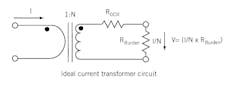
20-1. In the ideal current transformer ac current passes through the copper wind¬ings with very little resistive losses.
This indirect current measurement method requires a changing current, such as an AC, transient current, or switched DC; to provide a changing magnetic field that is magnetically coupled into the secondary windings (Fig. 20-1). The secondary measurement voltage can be scaled according to the turns ratio between the primary and secondary windings. This measurement method is considered “lossless” because the circuit current passes through the copper windings with very little resistive losses. However, a small amount of power is lost due to transformer losses from the burden resistor, core losses, and primary and secondary dc resistance.
Rogowski Coil
The Rogowski coil is similar to a current transformer in that a voltage is induced into a secondary coil that is proportional to the current flow through an isolated conductor. The exception is that the Rogowski coil (Fig. 20-2) is an air core design as opposed to the current transformer that relies upon a high permeability core, such as a laminated steel, to magnetically couple to a secondary winding.
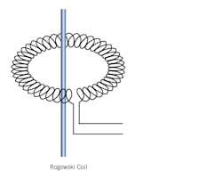
20-2. Rogowski coil is an air core design that has a lower inductance providing a faster response.
The air core design has a lower inductance providing a faster signal response and very linear signal voltage. Because of its design, it is often used as a temporary current measurement method on existing wiring such as a handheld meter. This could be considered a lower cost alternate to the current transformer.
Hall Effect
When a current carrying conductor is placed in a magnetic field, as shown in Fig. 20-3, a difference in potential occurs perpendicular to the magnetic field and the direction of current flow. This potential is proportional to the magnitude of the current flow. When there is no magnetic field and current flow exists, then there is no difference in potential. However, when a magnetic field and current flow exists the charges interact with the magnetic field, causing the current distribution to change, which creates the Hall voltage.
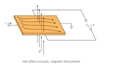
20-3. Hall-Effect devices are capable of measuring large currents.
The advantage of Hall effect devices is that they are capable of measuring large currents with low power dissipation. However, there are numerous drawbacks that can limit their use, including non-linear temperature drift requiring compensation, limited bandwidth, low range current detection requires a large offset voltage that can lead to error, susceptibility to external magnetic fields, and high cost.
Transistors
Transistors are considered a “lossless” overcurrent detection method since they are standard control components to the circuit design and no further resistance or power dissipating devices are required to provide a control signal. Transistor datasheets provide the on-resistance for the drain-to-source, {RDS(ON), with a typical resistance in the mΩ range for power MOSFETs (Fig. 20-4). This resistance comprises several components that begin with the leads connecting to the semiconductor die through the resistance that makes up the numerous channel characteristics. Based on this information, the current passing through the MOSFET can be determined by ILoad = VRDS(ON) / RDS(ON).
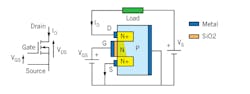
20-4. Power MOSFET’s on-resistance provides current sensing capability.
Each constituent of the} RDS(ON) contributes to measurement error that is due to minor variations in the resistances of the interface regions and TCR effects. The TCR effects can be partially compensated by measuring temperature and correcting the measured voltage with anticipated change in resistance due to temperature. Often times, the TCR for MOSFETs can be as large as 4000 ppm /°C, which is equivalent to a 40% change in resistance for 100°C rise. Generally, this method provides a signal with approximately 10% to 20% accuracy. Depending on the accuracy requirements, this may be an acceptable range for providing overcurrent protection.
Ratiometric Current Sense MOSFETs
The MOSFET consists of thousands of parallel transistor cells that reduce the on-resistance. The current sensing MOSFET shown in Fig. 20-5 uses a small portion of the parallel cells and connects to the common Gate and Drain, but separate Source. This creates a second isolated transistor; a “sense” transistor. When the transistor is turned on, the current through the sense transistor will be a ratio comparable to the main current through the other cells.
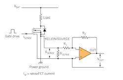
20-5. SenseFET uses a small portion of its parallel MOSFET cells to sense current.
Depending on the transistor product, the accuracy tolerance range can vary from as low as 5% or as wide as 15%-20%. This is not suitable for current control applications that typically require 1% measurement accuracy, but is intended for overcurrent and short circuit protection.
Resistor Technology Benefits
Thin film is not typically used for current sense applications, but is included in this discussion to provide breadth to the topic. Generally these resistive products are for precision applications because of the resistive layer ranges from 0.000001 in. to 0.000004 in. thick. They are quite surge-tolerant in the appropriate application, but are not designed for the high currents typically associated with the applications mentioned here.
Thick film, typically 0.0005 to 0.002 in. thick, is nearly 100 times thicker than thin Film. The increased thickness equates to a greater mass that is better able to carry the relatively high currents and dissipate the heat across the substrate, as well as better able to manage transients. Another advantage of the thick film products is the flexibility to request standard resistance values because of the process efficiency of laser trimming. The tradeoff of thick film is that these products are not as capable of the very tight tolerances of thin film products.
Foil technology has a larger cross section still and is a uniform resistive alloy, which is different from the thick-film technology that employs resistive materials suspended in a glass matrix. By comparison, the foils tend to withstand larger surge transients as compared to the previous versions. The principle advantage with this technology is the low range ohmic values with low TCRs.
Bulk alloy resistor technology has the greatest surge tolerance because of its large current carrying mass. It is available in resistance values as low as 0.000 5 Ω with low TCR. Bulk alloy tends to be the best choice for high current power supplies, or for where fault conditions can result in extreme currents. These products do not have as wide of a resistance offering as the Thick Film products, because the resistor alloy has limited resistivities to reach high range values, as well as needing the mechanical strength to tolerate process handling.
Product-Specific Features
High-current applications require the resistance value to be very low to minimize power losses and yet provide the necessary signal level to provide a voltage signal high enough to exceed noise levels. These low ohmic values often times need a four-terminal connection to reduce errors that may result due to the contact resistance that occurs when the part is mounted to the board.
The CSL (Fig. 20-6a) offers four terminals by design, but other standard surface-mount devices can benefit from a four-terminal pad design.
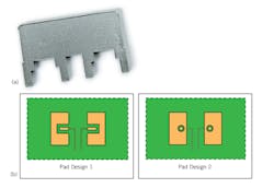
20-6a. Shows a four-terminal resistor for current sense applications.
20-6b. Two pad designs, (1) with isolated pad regions, and (2) with a plated through-hole.
These parts offer physically separated connection points for current and voltage, which reduces contact related measurement error. In the case of the CSL, the current will flow through the inner pins and voltage is sensed on the outer pins and is recommended for best accuracy with the LRF3W to be configured as a cross flow arrangement with current on diametrically opposing corners (e.g., pin 2 to pin 3).
The pad layout (Fig. 20-6b) creates separate regions for measuring signal voltage from the current carrying portion, which reduces error. Pad Design 1 illustrates one method that creates an isolated pad region within the pad layout, but this design may reduce the pad area below necessary limits to carry high currents through the copper trace. Pad Design 2 uses a plated through-hole to connect under the pad and connects to an internal or outer trace for measurement; this maximizes the pad space to carry current to the resistor. The contact point places the signal line as close to the current channel as possible; minimizing measurement error.
Thermal Isolation
The OARS (Open Air Resistor Surface Mount) is a unique design that elevates the hot spot of the resistive material well above the circuit-board material. This places the hottest region of the part into the available airstream, which dissipates the maximum amount of heat energy to the air instead of the PCB.
This provides two key advantages for thermal design, which affects the PCB material and the other neighboring power or semiconductor components. Typical FR4 PCB material is only rated to 130°C; a power resistor that is traditionally against the board could cause damage to the material during power excursions or reduces the upper temperature performance limits of the circuit. An elevated current sense prevents damage to the circuit material and permits the solder joint to run cooler. The second benefit by dissipating the heat to the air instead of the PCB is the improved performance of nearby heat-affected devices. These effects may include lifetime rating, power handling, luminous output, accuracy, and reliability.
The thermal images shown in Fig. 20-7 help illustrate the isolation performance of the OAR and OARS products.
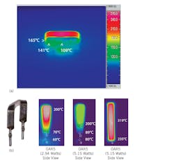
20-7. Thermal images illustrating the isolation performance of the OARand OARS product.
These tests were conducted on FR4 board material with no ambient airflow; airflow would improve system thermal performance. Observe the temperature of the solder joint with respect to the hot spot. These temperatures are based on reaching thermal equilibrium, however in the application these results may be extended to be considered as the thermal performance characteristics for an overcurrent protection condition. The FR4 will not exceed its temperature rating, though extreme circuit conditions exist.
Solder Joint Stress
The OARS resistive product family’s elevated and curved construction permits the resistor to flex. This construction reduces the stress generated by differences in thermal expansion coefficients between the heat producing metal and the dissipating circuit board material. Surface-mount components that are flat and parallel to the circuit board will apply shear forces to the solder joint that can lead to failure or changes in performance. In high thermal cycling applications, the OARS has been preferred to other similar all-metal construction parts because of this flexibility feature (Fig. 20-8).
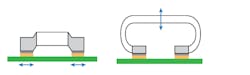
Figure 20-8. Differences in the thermal expansion coefficient between the metal materials of the current sense resistor and the circuit board materials dissipate forces on each part.
The LRF3W (Fig. 20-9) from TT electronics provides several design benefits derived from its 1225 aspect ratio with the termination along the long side of the component.
Figure 20-9. LRF3W from TT electronics uses side terminations to achieve a 3W rating.
The side termination extends the power rating to 3 Watts, eliminating the need to reduce the circuit traces as required by the traditional 2512 footprint. It also reduces solder joint stresses due to differences in the temperature coefficient of expansion between the ceramic and PCB material. The 1225 aspect ratio reduces the distance between the center / hot spot region of the part and the thermally dissipative circuit board material. This permits a high 3W rating and lessens the stress on the solder joint due to the differences in the temperature coefficients of expansion between the ceramic substrate and the thermal mass of the printed circuit board material.
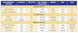
Table 20-1 compares the current measurement methods.
Read more articles from the Power Management Series in the Power Management section of our Series Library.

About the Author
Comment About the Article
To join the conversation, and become an exclusive member of Electronic Design, create an account today!

Leaders relevant to this article: