Power Management Chapter 24: Test and Measurement

This articles is part of the Power Management Series in the Power Management section of our Series Library.
Download this article as a .PDF eBook.
Power management involves test and measurement in three different levels:
- System
- Subsystem
- Component
At the system level, there are ac and dc power analyzers. At the subsystem level, a considerable amount of test and measurement systems can ensure a power supply is working properly. Testing at the component level mostly involves the power semiconductors employed in the system.
AC Power Glossary
RMS (Root mean squared value) is the most commonly used and useful means of specifying the value of both ac voltage and current. The RMS value of an ac waveform indicates the level of power that is available from that waveform, which is one of the most important attributes of any ac source.
RMS value = Peak Value/√2
Crest Factor is the relationship between peak and RMS.
Crest Factor = Peak Value/RMS Value
For a sinusoid: Crest factor = √2
Because the output current of a switch-mode power supply is not sinusoidal, the crest factor of the current waveform can be much greater than √2
Average Value can only have real meaning over one half cycle of a symmetrical waveform.
Average Value= Area enclosed by one half cycle/Length of base over one half cycle
Real Power is the power available to the load to do real work and is given in Watts. With a pure resistive load, you can multiply the RMS voltage and RMS current to get real power.
Apparent Power equals the product of the RMS voltage and RMS current.
Apparent Power= VRMS Y= IRMS
Reactive Power is the vector difference between Apparent Power and Real Power and is measured in Volt-Amperes (VA). This is correct for sinusoidal waveforms.
Power Factor for sinusoidal voltage and current waveforms is the cosine of the phase angle (θ) between the voltage and current waveforms.
Power Factor = Real Power/Apparent Power
Harmonic Distortion on an ac powerline is a non-sinusoidal current waveform that consists of a fundamental component at the supply frequency plus a series of harmonic frequencies that are integral multiples of the fundamental frequency (Fourier Analysis).
Total Harmonic Distortion (THD) is a figure of merit that quantifies the level of harmonics in non-sinusoidal ac voltage or current waveforms.
System: AC and DC Power Analyzers
Power analyzers accurately measure electrical power characteristics of devices that generate, convert, or consume electricity. There are now two types of power analyzers: ac and dc. A dc power analyzer allows engineers to gather and configure multiple instruments to complete dc sourcing and measurement tasks. AC power analyzers provide precise measurements of true power (watts), power factor, harmonics and efficiency in power-conversion equipment. Reliable ac power analyzers enable engineers to minimize energy loss due to distorted, transient waveforms in power electronics such as inverters, motors, lighting circuits, and power supplies.
Engineers working on electronic power-conversion systems need high-accuracy measurements to identify and characterize incremental efficiency improvements. Precision ac power analyzers offer high accuracy and ease of connection to the DUT, making them ideal for steady-state measurements of power consumption, efficiency, and power quality. For these measurements, the accuracy of the power analyzer gives R&D engineers the measurement integrity they need. With floating inputs and directly connected measurements, precision power analyzers make it easy for engineers to connect to their DUTs.
Traditionally, only oscilloscopes offer the single-shot measurement capability necessary for dynamic measurements during functional test. Furthermore, by offering a visual picture of what is happening, oscilloscopes allow engineers to gain insight into their DUTs and to identify issues. However, their lower accuracy means that making critical efficiency measurements on high-efficiency converters may be impossible. Because oscilloscopes have ground-referenced, non-isolated front ends, probes are required for floating and current measurements. Probes further reduce measurement accuracy and make oscilloscopes harder to connect to the DUT for high-accuracy, power-related measurements.
R&D engineers may have to switch between these two instruments depending on the type of measurement they need to make. They would use a power analyzer to make accurate measurements and an oscilloscope to visualize repetitive and single-shot events such as turn-on and occurrences of transients.
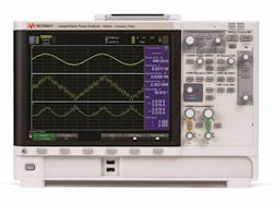
24-1. The Keysight Integravision ac power analyzer provides oscilloscope-like ability and ac power analysis.
Keysight’s PA2000 Series ac power analyzer provides oscilloscope-like ability and ac power analysis (Fig. 24-1). It supports the capture of voltage, current, and power waveforms over specific periods of time, with measurements made based on cursors placed on the captured waveforms. This helps in examining transient phenomena and in the design of periodically controlled equipment. To ensure that the DUT complies with energy standards, for instance, it is vital to measure power consumption across a range of different modes from sleep to full activity—and all the transient states in between.
Abnormal phenomena can often be hard to isolate, disappearing from the screen almost as soon as they appear. Like a traditional oscilloscope, you can set up the PA2000 ac power analyzer to make single-shot measurements to capture and measure transient phenomena, including in-rush, cycle dropouts, blackouts/brownouts, and other line disturbances.
Power analyzers use mathematical transformations to analyze signals. For precision, the measurement window cannot have any discontinuities or gaps. Continuous Whole-Cycle Analysis (CWA) used by the PA2000 Series is a gapless measurement technique that always performs measurements on a positive integer number of signal cycles.
Tektronix’ PA3000 is a one- to four-channel power analyzer optimized for testing single- and multi-phase, high-efficiency power-conversion products and designs (Fig. 24-2). Use it to quickly visualize, analyze, and document power efficiency, energy consumption, and electrical performance to the latest regional and international standards, including Level VI, EnergyStar, CEC, IEC 62301, CQC-3146, and more.
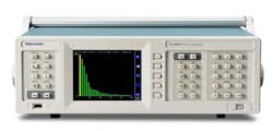
24-2. The Tektronix PA3000 is a one- to four-channel power analyzer optimized for testing single- and multi-phase, high-efficiency power-conversion products and designs.
Key features
- One to four channels support single- and three-phase applications
- 10 mW standby power measurement
- 1 MHz bandwidth
- 1 MS/s sampling rate
- 16 bit A/D
- Harmonic analysis to 100th order ±0.04% basic voltage and current accuracy
- Measurements to 30 Arms and 600 Vrms Cat II (2000 Vpk)
- USB and LAN interfaces standard (GPIB option)
- Free PWRVIEW software
- Full color graphical display for intuitive readouts of measured values, waveforms, harmonics, and energy integration plots.
The essential power-measurement tool for R&D and validation
- High accuracy supports testing to Level VI efficiency standards for external ac/dc power supplies
- Dedicated energy consumption testing in integration mode for standards like Energy Star and CEC
- Complete solution for full compliance testing to IEC 62301 standby power requirements
- 1 MHz bandwidth supports the LED module energy certification requirements of CQC-3146 as well as harmonic analysis of designs with higher fundamental frequencies
- More than 50 standard measurement functions, including harmonics, frequency, and star-delta computation
- Multiple analog and digital inputs for sensor data such as thermocouples, speeds sensors, and torques sensors.
- Built-in ±15 V supplies for external transducers to support high-current applications.
Applications
- AC/DC power supplies and LED drivers
- Appliances and consumer electronics
- UPS systems, inverters, and dc/ac conversion systems
- Wireless battery charging
- Three phase motors and drives.
Keysight’s N6705 DC Power Analyzer represents an entirely new instrument category for R&D engineers (Fig. 24-3). It provides productivity gains when sourcing and measuring dc voltage and current into a DUT. Using the N6705 DC Power Analyzer, R&D engineers can gain insights into the DUT’s power consumption in minutes without writing a single line of code. It provides an easy-to-use interface, with all sourcing and measuring functions available from the front panel.
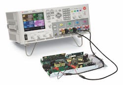
24-3. Keysight’s N6705 DC Power Analyzer provides insights into the DUT’s power consumption in minutes without writing a single line of code.
When executing these complex tasks, which can involve simultaneously connecting to and physically interacting with multiple test instruments, the risk of error increases. In response, R&D engineers may choose to automate tests that are too complex to do manually. Unfortunately, while automating tasks reduces human error, writing and debugging programs adds more work to already overloaded R&D engineers.
The N6705 DC power analyzer makes measurement tasks easy, right from the front panel:
- Set up and view critical turn-on/turn-off sequences.
- Measure and display voltage, current versus time to visualize power into the DUT.
- Control dc bias supply ramp-up/down rates.
- Generate dc bias supply transients and disturbances (arbs).
- Log data for seconds, minutes, hours, or even days to see current/power consumption or capture anomalies.
- Save data and screen shots to internal storage or external USB memory devices.
- Save and name your setup and tests for easy reuse.
- Share setups with colleagues.
The Keysight 14585A control and analysis software is a companion PC application that lets you control any of the N6700 family’s dc power modules when installed in up to four N6705 mainframes from a single PC control screen. This software provides improved data visualization and data management.
Subsystem: Power Supply Testing Test Probes
Designing a power supply requires the testing of various parameters to ensure its proper operation and that it meets system specifications. In addition, some of the same measurements must be employed in troubleshooting a defective power supply. In most cases, these measurements must be made without influencing the performance of the circuit under test.
Along with a vector network analyzer (VNA) and the appropriate probes, you can measure power supply parameters, non-invasively. The probes work for regulators, POLs, converters, and voltage references.
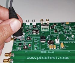
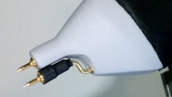
24-4. Picotest’s 1-Port probe is used to make an output impedance measurement of a voltage reference.
Picotest probes are referred to as PDN probes because they can measure low and ultra-low impedances found in Power Distribution Networks. PDN probes are 50Ω passive transmission-line probes. Their small and lightweight probe heads are intended for easy handling and high-performance measurement. The small form-factor probe tip and variable pitch ground lead allow designers to easily browse different device outputs, component footprints, and test points. There are two types of probes, the 1-port (Fig. 24-4) and 2-port (Fig. 24-5).
24-5. The Picotest 2-port probe.
Transmission line probes are a special class of passive probe that use a precision transmission line to replace the high-impedance probe cable, found in a traditional passive probe. The probe characteristic impedance matches the 50Ω impedance of a VNA or oscilloscope’s input. This reduces the input capacitance to a fraction of a picofarad, minimizing the loading of sensitive outputs with high-frequency signals.
Input impedance of the Picotest probes remain nearly constant over their entire frequency range, whereas a traditional ÷10 passive probe has a high input impedance at dc and drops rapidly with frequency, passing below the input impedance of a transmission line probe at <100MHz.
Transmission-line probes are useful in applications that produce fast-rising, narrow pulses with amplitudes that exceed the dynamic range of active probes. They also tend to have less parasitic effects on frequency response and so they are ideal for measuring impedance. By providing a simple, elegant, and flexible solution to probing high-frequency signals, Picotest’s 1- and 2-Port probes preserve signal fidelity and allow high-bandwidth test equipment to properly measure circuit characteristics.
The PDN probes have a wide dynamic range and can measure levels up to 5 V (RMS) without distortion. Their low inherent noise enables measurement of small signal levels. The comprehensive accessory set allows these probes to be connected to a wide variety of DUTs without impairing their very high bandwidth, though the length of the ground lead should be kept as short as possible.
High-speed applications put pressure on the measurement of power-supply buses to unprecedented frequencies. As an example, the measurement of PDN impedance for FPGAs, ASICs, and high-speed digital devices generally requires the measurement of impedance levels in the milliohm scale at frequencies exceeding 1GHz. Measuring the high-speed step-load response in power systems using 2-ports is difficult because of the need to connect two 50Ω transmission lines to the output capacitor. Compounding this difficult task is that these measurements often need to be made on very small circuits such as cell phones, solid-state disk drives, and computer tablets, etc.
These PDN probes are bi-directional. They can be used like a traditional probe to record signals or used to inject stimulus. For example, you can use a 1-port probe to inject a wide-band signal into your power rails in order to look for power-plane resonances or troubleshoot EMI problems. The 2-port probe can be used to transmit a stepped-load current pulse through one port, while measuring the voltage response from the other port, simultaneously.
These probes alleviate many physical testing challenges associated with traditional probes while maintaining precision 50Ω characteristics for a wide variety of measurements.
Among the important power-supply functional measurements are:
- Control loop stability
- Power supply rejection ratio (PSRR)
- Ripple and noise
- Bandwidth
- Rise time
- Output impedance.
Electronic Loads
An electronic load is a test instrument that emulates dc or ac resistance loads normally required to perform functional tests of batteries, power supplies, or solar cells. Programmability allows tests like load regulation, battery-discharge curve measurement, and transient tests can be fully automated and load changes for these tests can be made without introducing switching transient that might change the measurement or operation of the power source under test.
The electronic load electrically “looks like”a programmable resistor. These most commonly use one transistor/FET, or an array of parallel connected transistors/FETs for more current handling, to act as a variable resistor. Internal circuitry in the equipment monitors the actual current through the transistor/FET, compares it to a user-programmed desired current, and through an error amplifier changes the drive voltage to the transistor/FET to dynamically change its resistance. This negative feedback results in the actual current always matching the programmed desired current, regardless of other changes in the supplied voltage or other variables. Most commercial dc loads are equipped with microprocessor front-end circuits that allow the user to not only program a desired current through the load (constant current, or CC), but the user can alternatively program the load to have a constant resistance (CR) or constant power dissipation (CP).
24-6. Chroma System Solutions’ 63200 electronic load.
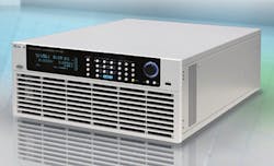
Chroma System Solutions’ 63200A (Fig. 24-6) is a high-power electronic load intended for testing power-conversion products including ac/dc and server power supplies, dc/dc converters, EV batteries, automotive charging stations, and other power electronics components. Built-in digital signal microprocessors (200MHz) provide optimal speed and control performance. These loads can be synchronously paralleled and dynamically synchronized for generating complex multi-channel transient profiles. The 300% peak overpower capability provides extra headroom for fault-condition simulations in automotive batteries and fuel cells.
Advantages of the 63200A series include ultra-high density power (6kW@4U), built-in digital microprocessors, master/slave parallel control, sine wave dynamic loading, and an industry leading measurement accuracy achieving 0.015%+0.015% F.S., 0.04%+0.04% F.S., and 0.1%+0.1% F.S. accuracy for voltage, current, and power measurement, respectively.
The front panel includes iconic function selectors via rotary knob or arrow keys and a vacuum fluorescent display. For pain-free viewing and access, the entire front panel tilts upward on 7U, 10U, and 13U models. Operation can be achieved by the front panel or from a remote workstation via standard USB or optional Ethernet and GPIB interfaces.
The 63200A series is complete with 150V, 600V, and 1200V voltage ranges and 3kW to 24kW power ranges. The maximum current of a single unit is 2000A and up to 480kW when paralleled. These high-power dc electronic loads are designed for testing server power supplies, A/D power supplies, batteries and energy storage systems, EV/EVSE, solar, and other power electronics.
Components: Power Semiconductors
Typical power semiconductor data sheets usually describe device behavior, but only over a limited range of operating conditions. This makes the operating conditions even more complicated because improved power MOSFETs and IGBTs can now operate at several hundred volts and hundreds of amps. This challenges the designer to obtain his/her own accurate power device measurement data over a broader range of operating conditions than those provided in data sheets.
Test measurements necessary to support the choice of the optimum power MOSFET in terms of power dissipation, reliability and efficiency, include:
- Static characterization (breakdown, RDS(ON), leakage, etc.)
- Characterization based on bias and temperature conditions experienced by devices in the actual end item system
- Drain (collector) voltage dependency of FET junction capacitances
- Gate charge characteristics
- Power losses.
For best results, use a test instrument that provides wide current and voltage measurements. To minimize device heating, testing the power semiconductor at high currents must be done using a series of short pulses. Fig. 24-7 shows a typical a plot of IC vs, VCE and Fig. 24-8 shows the breakdown voltage characteristics of a power MOSFET.
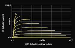
24-7. Typical plot of IC vs. VCE presented on a Keysight B1506A.
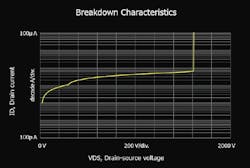
24-8. Breakdown characteristics of a power MOSFET presented on a Keysight B1506A.
Although no current should flow in the off-state of high-power applications, there can often be small leakage currents. This means that even sub-nanoamp current measurements on the power devices may be necessary to guarantee the energy efficiency of the end product. Understanding the maximum current when a device is on and the leakage current when a device is off is important because the test instrument must be able to measure currents as low as picoamps and voltages as low as microvolts as well as much higher operating currents and voltages.
Besides measuring general device characteristics over temperature, the designer may also want to screen various devices because they can look fine at room temperature, but be out of spec at a low or high temperature. Unfortunately, temperature characterization of power devices is not easy. Special measurement techniques must be used because these tests require a thermal test chamber whose temperature can take a long time to stabilize, and long cables leading from the chamber to the test equipment can create resistive and inductive oscillation problems. And, some applications may require performing device tests at temperature extremes, such as -50°C to 250°C. Fig. 24-9 is an example of temperature dependence of a power MOSFET that shows the variation of on-resistance vs. temperature.
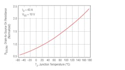
24-9. Variation of on-resistance (RDS(ON)) vs. temperature presented on a Keysight B1506A.
For all levels of current and voltage, it is important to obtain accurate and reliable measurement results. The larger the measurement error is in device evaluation, the larger the negative impact it has on circuit operating margins and peripheral circuit design. However, test data taken using traditional power device measurement equipment (such as curve tracers) is suspect in terms of measurement accuracy and reliability. Therefore, many circuit designers only use curve tracers to verify gross device functionality, and take the numerical measurement results as only a rough indication of device behavior. Obviously, when the need arises to compare the characteristics of multiple devices or to verify whether a device meets a manufacturer’s specifications, an approximate device characterization data is not meaningful.
A key parameter to determine from testing is total gate charge (QG), which is the total amount of charge necessary to turn on a power MOSFET. It is an extremely important parameter when estimating the driving loss during circuit operation. The driving loss consists of the product of QG, the gate voltage (VG), and the switching frequency. Accurate QG evaluation allows precise driving loss calculation as well as optimized design of the driving circuit. Fig. 24-10 shows a plot of VGS (gate-source voltage) vs. QG for a super junction MOSFET.
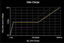
24-10. VGS (gate-source voltage) of a super junction MOSFET that indicates QG presented on a Keysight B1506A.
QG also provides other useful information to help with switching operation analysis. For example, when a circuit does not meeting performance expectations, examining the QG curve can offer valuable insights that identify the source of the problem.
Because QG varies with the output voltage and current, it should be evaluated under in-circuit bias conditions. The QG characteristics shown on a device data sheet only provides an approximation of the value of QG during actual circuit operation. Therefore, a designer must be able to accurately evaluate QG for both low voltage and high voltage power devices.
Besides driving loss, the designer may want to calculate conduction loss and switching loss. The QG curve can also be interpreted as a representation of the non-linearity of a power device’s stray capacitances. This makes it possible to calculate switching parameters and switching loss using known equations that combine the gate resistance, the resistance in series to the gate, and the switching frequency. The test instrument should have the ability to accurately measure on-resistance, RDS(ON), and peak current, and also calculate conduction loss. These calculations should be performed automatically by the test instrument for a given frequency.
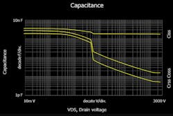
Understanding the input, output, and reverse return capacitances of three terminal devices (such as MOSFETs or IGBTs) is important, because these parameters dictate the switching speed and the switching loss when operating at high frequency. However, accurately measuring these parameters is not easy or straightforward. To make an accurate measurement, the capacitance between two terminals of a three terminal device, the other terminal needs to be appropriately configured.
It would be helpful if the test instrument automatically and accurately measures FET capacitance values (CISS, COSS, CRSS). This involves using all the resistors, capacitors, and protection circuits necessary to make high-voltage capacitance measurements. Fig. 24-11 shows a typical presentation of these capacitance values.
24-13. Keysight’s’ B1505A is a power-device analyzer/curve tracer for high-power semiconductors.
One test equipment for use with GaN and SiC transistors is Tektronix/Keithley’s Parametric Curve Tracer, specifically designed for high voltage and current characterization of high-power semiconductors. To meet the requirements of the new generation of high-power semiconductors, Keysight has enhanced its B1505A Power Device Analyzer/Curve Tracer to significantly increase its voltage and current range, allowing it to test GaN and SiC transistors (Fig. 24-13).
The enhanced B1505A Power Device Analyzer/Curve Tracer can measure a device’s characteristics from sub-pA up to 10 kV/1500 A, with a fast pulse down to 10 microseconds. Keysight also introduced the B1505AP, a preconfigured version of the B1505A that includes all modules, cables, and accessories necessary to ensure a quick startup. Both the enhanced B1505A and new B1505AP are intended for power-device researchers and manufacturers performing power-device characterization and failure analysis. These instruments can also be used for incoming device inspection and failure analysis.
Other features of the B1505A include:
- All-in-one solution for power-device characterization up to 1500 A & 10 kV
- Medium current measurement with high voltage bias (e.g., 500 mA at 1200 V)
- μΩ on-resistance measurement capability
- Accurate, sub-picoamp level, current measurement at high-voltage bias
- Capacitance measurement at up to ±3 kV DC bias
- 10μs high power-pulse measurement
- Temperature measurement capability
- High voltage/high current fast switch option for GaN current collapse effect characterization
- Automatically switch between high-voltage and high-current measurements without re-cabling
- Standard test fixtures with safety interlock for packaged power device testing
- Tested and supported high-power 200 A on-wafer testing
- MS Windows-based EasyEXPERT software simplifies data management and data analysis
- 10 module slots
- Support for high-power devices with up to six connection pins.
A curve tracer, such as the B1505A, produces I-V (current-voltage) curves that provide a good assessment of device behavior. Therefore, a curve tracer is the ideal instrument to determine the characteristics of these high-power, discrete semiconductors. Characterization of SiC and GaN devices requires an appropriate curve tracer with high breakdown voltage measurement capability as well as the ability to measure leakage currents at high voltage biases.
A GaN and SiC curve tracer needs a switch to automatically change the measurement resource between high voltage and high current. Otherwise, the operator must change measurement equipment connections to the device-under-test manually, which can cause trouble.
For best reliability results, I-V characteristics near the safe operating area (SOA) are an important measurement for GaN and SiC devices. When a high voltage is applied to a device, its impedance can change rapidly and apply medium to high current through the device. Using a narrow test pulse (less than 50µs) prevents device self-heating that could impact accurate characterization.
When originally introduced, curve tracers were analog instruments that employed a CRT (cathode ray tube) display. Today, curve tracers have become digitized and use flat-panel LCDs to present data. Digital techniques now provide the ability to store measurement data and retrieve it.
Older test equipment is not adequate for GaN and SiC because leakage current and breakdown voltage determine basic GaN and SiC behavior. Older test equipment, typically limited to the µA level, lacks sufficient resolution and accuracy for leakage characterization. And, if the breakdown voltage is more than 3kV, older instruments can’t even measure it. Companies have had to design and build a custom test system to measure ultra-high voltage. However, these may have safety and traceability issues.
GaN and SiC on-resistance is now as low as a few milliohms and continues to decrease, which causes measurement accuracy problems. Accurate measurement of on-resistance requires precise constant current applied to the device using an accurate voltmeter with a full Kelvin connection. Older-generation curve tracers don’t have current source capability, which makes it difficult to accurately perform characterization.
A current source mode can aid in accurately measuring GaN and SiC on-resistance. This requires continuous monitoring and adjustments for the internal feedback circuit used by the current source. This way, set current flows regardless of contact resistance variations and you can measure on-resistance very accurately. In contrast, a voltage source mode for the on-resistance test involves immeasurable contact resistance that causes a voltage drop and degrades the measurement. Pulsed current testing can help control the effects of device self-heating.
Test instruments can make on-wafer measurements. On-wafer measurements require extension cables to connect the test equipment and prober. In this case, the drive voltage has to be high enough to overcome the IR voltage drop in the extension cable. The GaN or SiC drain or collector supply voltage must have enough margin even when IR voltage drop is high due to high current. To ensure sufficient drive-supply voltage requires a special extension cable with low residual resistance. High-voltage testing at the wafer level requires a properly designed safety system to prevent the user from exposure to the high voltage. Interlock mechanisms between the prober and the instruments must be used to protect the user.
24-14. Keysight’s’ B1506A is a power-device analyzer/curve tracer for high-power semiconductors.
A proper test-fixture solution is extremely important, both to insure safety (due to the high voltages and currents used) and to support the wide variety of power-device package types. Fig. 24-14 shows the Keysight B1506A with a test fixture for a device under test. A previous limitation of curve tracers was that some power devices could not be evaluated due to their size, or it was necessary to jury-rig an adapter in order to test the device. Therefore, you need a test fixture that can accept a wide variety of devices, regardless of their size or shape so the test-fixture adapter must be customizable. In addition, the test fixture should have a built-in interlock mechanism to ensure that high voltages and currents do not endanger the device-under-test or the test operator.
One complication is that the existing GaN and SiC semiconductors require unique test fixtures because they may be housed in different packages. Plus, some of the GaN devices are enhanced mode and others are depletion mode with integrated driver circuits. Existing SiC devices now use industry-standard packages, but as their portfolio grows, newer packages will certainly have to be optimized for high-speed, high-power switching.
Safety is a concern when configuring any high-voltage test system. Typically, the test systems require safety interlocks, double grounds, and other safety features to protect operators and sensitive system instrumentation. In Europe, it requires test and measurement equipment to demonstrate safety by complying with EN61010-1. Internationally it is IEC61010-1 and in the United States it is UL61010-1.
Making Low-Current Measurements in Electronic Systems
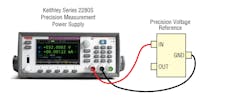
In the previous section we were concerned about high current and high voltage. We’ll move to the extreme with an application note from Tektronix) that describes how to make accurate measurement of low currents using a Precision Measurement DC Power Supply. The application note is Making Low Current Measurements with a Series 2280S Precision Measurement DC Power Supply.
Minimizing the power consumption of integrated circuits and electronic sub-assemblies is a major focus for manufacturers of these components. This means minimizing the current drawn by all integrated circuits and electronic subassemblies.
In the past, power consumption could be measured with a standard digital multimeter (DMM). Today, devices can have operating currents as low as microamps or less and require more sophisticated measurement equipment.
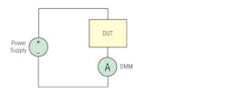
24-15. Measuring low current on a DUT using a power supply with a precision DMM in series with the DUT.
One way to measure low current on a low-power device under test (DUT) is to use a power supply with a precision DMM in series with the DUT, as shown in Fig. 24-15. With a quality 6½-digit DMM, accurate current measurements can be made at microamp levels. Although this method can provide accurate measurement of current through the device, it can also introduce problems due to the loading of the DMM.
Even though the voltage at the output of the power supply may be at the programmed value, the voltage at the DUT is actually lower than the programmed value due to the loading of the DMM. Rather than the programmed voltage, the voltage seen at the DUT’s terminals is equal to the programmed voltage minus the voltage across the DMM (VDUT = VSET – VDMM). If this voltage drop is not accounted for and the user assumes the voltage at the device is equal to the programmed voltage, then power and resistance measurements will have significant error because the voltage used to calculate them will be higher than the value at the DUT. This drop in voltage can also cause problems when testing the device at voltages near the minimum operating voltage. If the loading of the DMM is too great, the voltage seen at the device may be below the minimum operating voltage and the device will fail to operate correctly, resulting in incorrect measurements.
This drop in voltage could be compensated for by outputting a higher voltage at the power supply so the desired voltage appears at the DUT. However, the loading of the DMM varies with the amount of current flowing, so compensation is difficult. A second DMM could be used to measure the voltage at the device directly, but this not only adds cost and complexity to the test system by introducing yet another piece of equipment, it can also create a significant error source for low-current measurements. The DMM adds additional load to the test circuit, resulting in currents higher than those actually flowing through the device.
Using a Precision-Measurement Power Supply
A better way to measure the current is to use a precision-measurement power supply. The current through a device can be measured with the same precision as a high-quality 6½-digit DMM, but it can be done more simply and more accurately as well. Testing is simplified because only a single instrument is required to test the device.
With only a single instrument, testing can begin sooner because there is less equipment to set up. Automating the measurement is simpler as well with only one instrument to program. This eliminates the need to synchronize multiple instruments and allows the test engineer to focus on making the measurement.
Precision-measurement power supplies are capable of measuring both the current and voltage applied to the device. Current is measured internally, so it places no loading on the test circuit like a series DMM would. This results in the voltage at the device being equal to the programmed voltage.
For even greater accuracy, voltage can be sensed directly at the device using remote sense leads placed at the device terminals, allowing the precision-measurement power supply to compensate automatically for any voltage drops across the test leads that supply current to the device. These sense leads have very high input impedance, so they place virtually zero load on the test circuit. Using these features, precision-measurement power supplies are capable of performing very accurate characterization of devices at any current level. By containing all of this capability in one instrument, precision-measurement power supplies greatly decrease test system complexity as well as cost.
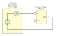
24-16. Precision-measurement power supplies reduce the amount of equipment necessary to make a low-current measurement on a device.
Read more articles from the Power Management Series in the Power Management section of our Series Library.
About the Author

Sam Davis
Sam Davis was the editor-in-chief of Power Electronics Technology magazine and website that is now part of Electronic Design. He has 18 years experience in electronic engineering design and management, six years in public relations and 25 years as a trade press editor. He holds a BSEE from Case-Western Reserve University, and did graduate work at the same school and UCLA. Sam was the editor for PCIM, the predecessor to Power Electronics Technology, from 1984 to 2004. His engineering experience includes circuit and system design for Litton Systems, Bunker-Ramo, Rocketdyne, and Clevite Corporation.. Design tasks included analog circuits, display systems, power supplies, underwater ordnance systems, and test systems. He also served as a program manager for a Litton Systems Navy program.
Sam is the author of Computer Data Displays, a book published by Prentice-Hall in the U.S. and Japan in 1969. He is also a recipient of the Jesse Neal Award for trade press editorial excellence, and has one patent for naval ship construction that simplifies electronic system integration.
You can also check out his Power Electronics blog.
Comment About the Article
To join the conversation, and become an exclusive member of Electronic Design, create an account today!

Leaders relevant to this article: