Download this article in PDF format.
In February 2019, my friend and mentor Jerry Dale Merryman passed away. He was most well-known for inventing the first digital handheld calculator known as “Cal-Tech,” which now resides in the Smithsonian in Washington, D.C. I first met Jerry at a TI Vets meeting I attended with my grandfather James R. “Bob” Biard. They had worked together in the 1960s at Texas Instruments (TI) in Dallas, Texas. I remember my grandfather used to tell me how he thought Jerry was the smartest engineer he had ever worked with.
Thomas M. Okon, COMPLEAT Implementations Team Lead at Concur
Within a short amount of time of meeting Jerry, it was clear to me why he held him in such high regard. It was, as Ed Millis stated in his 2008 biography on Nobel Prize winner Jack S. Kilby, Jerry was “the ultimate polymath”.1 At the TI Vets meeting, Jerry was at the center of a captivated audience and I was an avid listener. One story he told about working on a project with my grandfather, before being recruited for the Cal-Tech calculator project, really caught my attention. Over the next few years, it became a frequent talking point for all of us. I am very grateful to them both for sharing their memories with me.
Where It All Began
In September 1961, Bob began what is thought to be the first full-time project in the U.S. on gallium-arsenide (GaAs) light emitters (LEDs), after discovering that diffused GaAs diodes emitted near-infrared light and could be used in optoelectronic applications. A few months later, Bob and his former Texas A&M professor, Walter T. “Walt” Matzen, initiated a contract with the U. S. Air Force to study the piezoelectric, thermal, and optoelectronic interactions in semiconductors in order to extend the capability of functional electronic blocks (FEBs).2
As part of the study for the Air Force, Bob, Jack Kilby, Edward L. “Ed” Bonin, and Gary E. Pittman investigated the use of optical coupling as an alternative solution to transformers, for breaking up ground loops in interconnected pieces of electronic equipment. During the early 1960s, transformers were often bulky, had limited bandwidth, and were ineffective for dc signals.4
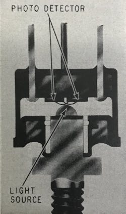
The first such device they developed was an Optoelectronic Multiplex Switch, also known as a chopper. The device consisted of two silicon phototransistors illuminated by a single, GaAs dome LED (Fig. 1).3 The chopper device, marketed as the PEX3002 and PEX3003, was officially announced as a commercial device in March 1964. On Nov. 29, 1963, they filed a patent titled “Photosensitive Transistor Chopper Using Light Emissive Diode” based on their device. U.S. Patent 3,304,431 issued on Feb. 14, 1967. 5
1. Cross-sectional view of a four-terminal switch with a GaAs dome LED coupled to two phototransistors.3
It was in February 1963, while employed at Texas Research Electronic (TRE), Jerry attended the International Solid-State Circuits Conference at the University of Pennsylvania. He was there in Session IV: Low-Frequency Circuits to present a paper on a liquid-state dc amplifier using solion tetrodes with a dc gain of 500.6 According to Jerry, at the conference he remembered being a country boy in a big new world and didn’t expect to know anyone.
Although they did not cross paths at the conference, two days later in Session XII: Optoelectronics, Bob and his TI co-workers presented a paper regarding the use of GaAs LEDs for optoelectronic applications.7 It was the following month that Jerry applied for a job at TI and was hired to work in the IC Dept. in the Semiconductor-Components (SC) Division. According to Jerry, Walt Matzen was his mentor at TI. Walt taught him about integrated circuits on his first day there.
The Initial Design
In late 1963, Jerry was in the group making silicon integrated circuits and Bob’s group was making GaAs light emitters, so an opportunity for collaboration presented itself. Bob approached Jerry and suggested how they could make an optically coupled device using a Faraday shielded diode on a chip with an operational amplifier and a digital output electrically isolated from the input. Jerry thought it was a good idea and agreed to do it.
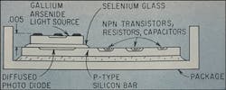
Jerry started by designing the layout, dimensions, and metallization pattern for the device. It consisted of a planar, flat, zinc-diffused GaAs diode bonded to a p-type silicon chip using selenium glass (Fig. 2). The selenium glass electrically isolated the GaAs diode from a diffused, n-type photodetector beneath it, while also acting as a medium for the transmission of near-infrared light to the photodiode.
2. Cross-sectional diagram of the optoelectronic pulse amplifier (OPA).4
Ray Hilton, in TI’s Semiconductor Exploration Laboratory, was the one who made the glass. They initially tried using a high-lead (Pb) glass because they knew the glass needed a high index of refraction and minimal light absorption. However, after fusing the GaAs and silicon at 450º C, they found the lead reduced the optical transmission. They then tried using a selenium-arsenic glass, but found the working temperature for the glass was too low for general usage of the device. 8 They wound up using a thin layer of selenium glass because it was very transparent in the near-infrared range. The optimum glass bond was formed using chalcogenide glass composed of selenium, germanium, and phosphorous.4
To reduce passivity, the GaAs diode was electrostatically shielded from above using a grounded aluminum sheet and a layer of oxide. When a forward-biased input current of 5 mA at 1.2 V was applied to the GaAs diode, it emitted near-infrared light at a wavelength of about 0.9 µm.
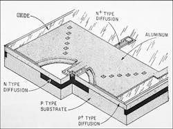
The light emitted from the p/n junction passed through the selenium glass, whereby it was absorbed by the silicon photodetector layer, which was diffused into the p-type substrate of the monolithic silicon chip. The photodetector consisted of emitter, base, and collector diffusion. The base and collector were used as a photodiode. The emitter diffusion, between the photodiode and selenium glass, consisted of a grounded, transparent, P+ type layer with a low sheet resistance to reduce distributed capacitance and spurious electrical coupling between the LED and the photodiode (Fig. 3).
3. Elevational view of the electrostatically shielded photodetector, partly cut away to show the inner composition.4
Upon absorption of the emitted light, the photodetector generated electron-hole pairs, which produced a photocurrent at the active junction of the photodetector. A narrow strip of the aluminum sheet above the GaAs diode extended down into the n-type layer of the photodiode as a further safeguard against high-frequency noise.
The Feedback-Amplifier Circuit
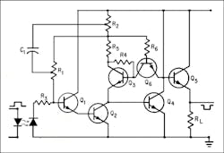
Since the photodiode’s output current was less than 1% of the drive current, a high-gain amplifier was required. For this, Jerry designed a multi-stage, pulse amplifier circuit consisting of diffused resistors, NPN transistors, and capacitors. He designed the input stage of the circuit as an operational amplifier by pairing transistors Q1 and Q2 (Fig. 4) with additional amplification provided by transistors Q4 and Q5.
4. OPA circuit diagram with inclusion of capacitor C1 connected to tap arrangements of resistor R1 and R2.4
To prevent saturation of the output stage, which could happen if the LED was over-driven, Jerry had to do some innovative circuit design. When you saturate a transistor, a lot of charge builds up and it takes time to pull the charge back out, which makes the transistor’s response time slow. To resolve this issue, Jerry designed a negative feedback network with half the output of the amplifier fed back to the middle of a high resistance feedback resistor (R1), which provided a low load resistance for the photodiode.
According to Jerry, the only feedback resistor you could get in an IC, at the time, was embedded in a semiconductor moat, which resulted in a large amount of distributed capacitance, high-frequency instability, and the possibility of oscillation. To eliminate such issues, Jerry added a tap on feedback resistor R1 and a tap on collector resistor R2, which connected to a 15-pF capacitor (C1). Transistors Q2, Q3, and Q6 were added in conjunction with resistors R4 and R6 to prevent saturation of transistor Q4. Q3 acted as an emitter-follower to prevent an increase in the collector potential of Q2, which in turn prevented saturation of Q4. The emitter of the output transistor Q5 connected to the output pin of the device’s package known as a flatpack.
When the output circuitry was connected to a 6-V power supply, the device produced 5-V digital pulses 200 ns later. Although designed for 6 V, it was shown to work at 3 V as well, albeit with smaller amplitudes and longer rise times.9
DIY Photomasking
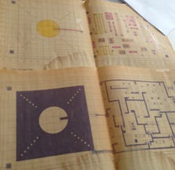
In the mid-1960s, TI fabricated ICs using a photomask process. According to Jerry, it was in large part, do-it-yourself. You would start off by drawing your design (Fig. 5) on graph paper, or engineer's quadrille pad, to fit the dimensions of a standard header. The design would then be drawn on a large, clear sheet of plastic called a peel-coat with a red film on it, which would be scored with a razor blade according to the design. The excess red film would then be torn off to make a negative.
5. Jerry’s original drawings of the OPA’s layout.
Subsequently, that would get photographed multiple times using a large Robertson camera on a rail mount to reduce the picture to the size of a postcard, approximately 30X larger than the final IC. After that, it would get photographed down to 5X or 10X the size of the final IC and printed on a glass called a reticle, which would then be placed into a stepping machine and further reduced. The ending image was shot vertically down onto a platen with a precision x-y transport using a step and repeat machine in order to make multiple copies of the bar.
Papers, Patents, and OPA SNX1304
On June 3, 1964, Bob presented a paper on “Optoelectronic Functional Electronic Blocks” before an audience of Air Force R&D personnel and industry representatives at Wright Patterson Air Force Base in Dayton, Ohio. On June 29, 1964, Bob and Jerry filed a patent (U.S. Patent 3,436,548) titled “Combination P-N Junction Light Emitter and Photocell Having Electrostatic Shielding.”10 They also filed a French patent (No. 1,452,104) for an “Electrostatically Shielded Optoelectronic Device.” which was issued on August 1, 1966.
In December 1964, Bob, Jerry, Walt, and Ed Bonin published a paper titled “Optoelectronics as Applied to Functional Electronic Blocks” in the Proceedings of the IEEE.11 On Feb. 18, 1965, Jerry presented a paper titled “An Optically-Coupled Digital Integrated Circuit” in Session VI: Radiative Interconnections at the University of Pennsylvania.9
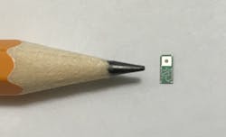
In March 1965, TI announced the SNX1304 as an experimental Optoelectronic Pulse Amplifier for engineering evaluation. The device, which is thought to be the first commercial optically coupled integrated circuit, was mounted in an opaque, 10-lead, hermetically sealed, TO-89, flat package, which measured 1/8 × 1/4 × 1/32 in. The approximate weight was 0.1 gram. The silicon chip measured 0.065 × 0.15 in. According to the TI bulletin, the device “functions as a broad-band pulse transformer with response extending to zero frequency”.12 The electrical isolation of the device provided rejection of common-mode noise attributed to ground loops in networked electronic equipment.
In July 1965, Jerry published an article in Electronics magazine describing the Optoelectronics Pulse Amplifier.4 Then in September of that year, Jerry was recruited by Jack Kilby for the Cal-Tech calculator project. The following month, Bob became Manager of the Compound Semiconductor Program in SRDL. It was around this time that Ed Bonin secured a contract with the Jet Propulsion Laboratory in Pasadena, Calif. to continue development of the SNX1304.
The project also included development of a new type of GaAs emitting diode-Si phototransistor pair called a GaAs switch, which became the PEX4001. In Ed’s second report, he described how inversion layers, which formed on the collector and base surfaces of the phototransistor in the GaAs switch, had resulted in large leakage currents.13 Bob came up with a solution incorporating an N+ diffusion (guard-ring) on the collector surrounding the base to eliminate the effects of the inversion layers. In December 1966, the Marshall Space Center published an article proposing use of the SNX1304 in the telemetry system of the Saturn V rocket in order to optically isolate the PCM/DDA system and the Computer Interface Unit (CIU).14
In the spring of 1967, Edgar E. “Ed” Harp transferred from TI's Central Research Lab (CRL) to Bob's group in the Optoelectronics branch. Under the direction of Ed Bonin, for the next year he worked on device development of the photon-coupled isolation switch. J.C. Lewis and W.A. “Dub” Little worked on the silicon diffusion. According to Ed Bonin’s final report in 1968, the SNX1304 became the TIXL106.15 The TIXL106 came in what they called a “mech-pak,” which was used for automatic machine insertion, as opposed to having to solder it down to a circuit board, as was the case with the flatpack.
Closing Thoughts and Memories
In April 2016, my grandfather and I decided to nominate Jerry for an honorary degree. In learning about Jerry’s career, he kindly shared with me a lot of the content of this article. I was surprised to learn he had saved his original drawings of the OPA layout (Fig. 5, again), oscilloscope curves showing input current vs. output current, and some of the silicon chips (example in Fig. 6) before addition of the GaAs diode.
6. Closeup of the OPA's silicon chip without the GaAs diode.
Using his microscope, I got to look at the OPA chip up close. Jerry explained to me that the different colors we could see were interferences caused by the different thicknesses of oxide due to the sequence of fabrication steps. I was surprised to learn the microscope was the one he had used while working on the Cal-Tech calculator.
According to Jerry, sometime in the mid-1960s, he was running a few slices and a few bars when an Air Force monitor had shown up to check on their progress. He came by and talked to Jerry and said, “How many of those bars did you make?” Jerry said “18,000.” The Air Force monitor replied, “We just needed the one to see if it would work.” And Jerry said, “Well, when you make an integrated circuit, you get a bunch of ‘em.”
Thomas Okon, COMPLEAT Implementations Team Lead at Concur, earned his B.S. in Computer Science from the University of North Texas in 2007. He is the grandson of LED inventor James R. Biard. In 2015, Thomas co-authored a paper with his grandfather about the development of LEDs at Texas Instruments in the 1960s. For the last year he has been mentored in the fields of physics and engineering by Jerry D. Merryman, the inventor of the first digital, handheld calculator.
References
1. E. G. Millis, Jack St. Clair Kilby, A Man of Few Words: A Brief Biography, Ed Millis Books; 2008.
2. W. T. Matzen, Ed., “Semiconductor Single-Crystal Circuit Development,” Texas Instruments Incorporated, Contract No. AF33(616)-6600, Rept. No. ASD-TDR-63-281; March 1963.
3. E. L. Bonin, “Light-coupled semiconductor switch for low-level multiplexing,” Electronics magazine, Vol. 38, No. 3, pp. 54-59; Feb. 8, 1965.
4. J. D. Merryman, “Making light of the noise problem,” Electronics magazine, Vol. 38, No. 15, pp. 52-56; July 1965.
5. J. R. Biard, E. L. Bonin, J. S. Kilby, and G. E. Pittman, Texas Instruments Inc., “Photosensitive transistor chopper using light emissive diode,” U.S. Patent 3,304,431; Issued: Feb. 14, 1967.
6. J. D. Merryman, “A low-level DC amplifier using solion tetrodes,” Solid-State Circuits Conference, Vol: 6, pp. 42-43; Feb. 1963.
7. J. R. Biard, E. L. Bonin, W. N. Carr, and G. E. Pittman, “GaAs Infrared Source for Optoelectronic Applications,” 1963 IEEE International Solid-State Circuits Conference, Volume 6, pp. 108-109; Feb. 1963.
8. J. R. Biard, “Optoelectronic Functional Electronic Blocks,” Interim Engineering Report No. 0464-20, Texas Instruments Inc., Dallas, TX; March 27, 1963.
9. J. D. Merryman, “An optically-coupled digital integrated circuit,” Solid-State Circuits Conference, Vol: 8, pp. 58-59; Feb. 1965.
10. J. R. Biard and J. D. Merryman, “Combination P-N junction light emitter and photocell having electrostatic shielding,” U. S. Patent 3,436,548, Issued: Apr. 1, 1969.
11. J. R. Biard, E. L. Bonin, W. T. Matzen, and J. D. Merryman, “Optoelectronics as Applied to Functional Electronic Blocks,” Proceedings of the IEEE, Volume: 52, No: 12, pp. 1529-1536; Dec. 1964.
12. “Type SNX1304 Optoelectronic Pulse Amplifier,” Texas Instruments Bulletin No. DL-S 657611; May 1965.
13. Texas Instruments Inc., “Photon Coupled Isolation Switch,” JPL Contract No. 951340, Second Quarterly Report, April 1-June 30, 1966.
14. T. C. Lawson, “Integrated Circuits In Telemetry Systems,” Electronic Research At MSFC, pp. 33-40; May 26, 1966.
15. Texas Instruments Inc., “Photon Coupled Isolation Switch,” JPL Contract No. 951340, Final Report, January 1, 1966-March 31, 1968.
About the Author
Thomas Okon
COMPLEAT Implementations Team Leader
Thomas Okon, a Senior Technical Consultant in the field of travel automation software, earned his B.S. in Computer Science from the University of North Texas in 2007. He is the grandson of LED inventor James R. Biard. In 2015, Thomas co-authored a paper with his grandfather about the development of LEDs at Texas Instruments in the 1960s. For the last year he has been mentored in the fields of physics and engineering by Jerry D. Merryman, the inventor of the first digital, handheld calculator.
