Analyze MOSFET Parameter Shifts Near Maximum Operating Temperature
Dealing with the inevitable heat dissipation of a discrete power transistor such as a MOSFET is an ongoing engineering problem. In many cases, a heatsink is the solution: the better the heatsink, the smaller the difference between the ambient temperature and the transistor die’s temperature. The optimal heatsink choice is a compromise between the size, cost, and required reliability.
This file type includes high resolution graphics and schematics when applicable.
But what happens to the MOSFET’s performance if the ambient temperature is close to the maximum temperature Tjmax in the manufacturer’s spec? Where is the breaking point? What do you do if the equipment using this MOSFET has to operate near the hot engine or in the hot oil well, where the ambient temperature can be above 150°C, 175°C, or even higher? How does the MOSFET behave, and how do the conduction losses change? Is there a sign of life behind the specified Tjmax?
Related Articles
- Determine MOSFET Junction Temperatures And Switching Losses For Various Package Types
- When Heat Is On, Thermal Characterization Keeps Things Cool
- Informed Analysis Picks Better 555 Timer To Drive Power MOSFET
By The Numbers
When the temperature rises, the drain-to-source voltage drop VDS increases significantly (Fig. 1). At the same time, it depends on the drain current.1
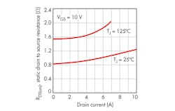
Manufacturers now provide excellent datasheets with the important reference data including RDS(on), measured at a specific test currents, ITest, for maximum pulse and maximum continuous currents, at 25°C and 150°C. This data usually is backed with a set of graphics showing the output drain characteristics, such as drain current Id versus drain voltage Vd and a static drain-source on resistance for 25°C and 150°C.
Figure 2 is an example of the combination of these two drain characteristics for the IPB60R099 MOSFET, based on the datasheet graphs.2
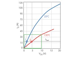
The blue curve represents the drain characteristic for 25°C. The red one is for 150°C. Both curves are for the 10-V gate voltage. The manufacturer’s datasheet also provides two RDS(on) values, measured at ITest = 18 A for 25°C and 150°C shown as small circles #1 (0.09 Ω) and #2 (0.23 Ω). Ratio K of voltage #2 to voltage #1 is an important thermal characteristic:
K = RDS(on)150°C/RDS(on)25°C (1)
Different transistors have different voltages and current ratings and respectively different values of ITest, of course.
In most cases, the MOSFET is used as a switch and its drain current is a parameter determined by other components and conditions, while its drain voltage is a function to be defined or calculated to find both momentary and average power dissipation. An analytical equation providing the momentary resistance value RDS(on) versus temperature and drain current would be very useful for evaluating the numbers using computer simulation.
The Design Note3 provides an equation for the dependence of RDS(on) on the temperature, but its current dependence was left out of picture:
RDS(on)T = RDS(on)(25°C)(T/300)2.3 (2)
where T is absolute temperature (K).
Reference 4 proposes methods to determine another equation for RDS(on) versus temperature, without current effects:
RDS(on) = RDS(on)(25°C)(a * Tj2 + b * Tj + c) (3)
Two expressions describing RDS(on)’s dependence on the temperature are available. One is a simple linear equation, and the other is a more precise second-order equation. However, neither of these includes an important current dependency.
This prompts two logical questions. First, do these equations cover all MOSFETs, or do MOSFETs with dissimilar maximum-voltage ratings behave differently? Second, how can at least one of these equations be modified or improved to add a current as a second parameter?
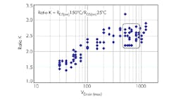
The first question was answered using a sophisticated Monte Carlo method. It took considerable time to gather the information from the datasheets for several groups of MOSFETs with maximum drain voltages from 30 V to 1200 V and then to calculate K for each group. Figure 3 shows a scatter plot of K versus maximum drain-voltage rating.
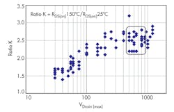
The trend in the data clearly indicates that K depends on the MOSFET’s maximum voltage rating Vd and K changes from ≈1.5 for low-voltage transistors to ≈2.9 for high-voltage ones.
The power value P in Equation 2 can be 2.3 only for certain MOSFETs (Fig. 4).
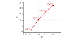
Due to the author’s involvement in the practical designs for power buses in the range of 400 V to 600 V range, the group of interest was narrowed down to the 600-V to 900-V range of the maximum drain-voltage ratings (green zone, Figure 3).
The next steps were to use these common-sense assumptions:
• Make it simple. For room temperature, use a linear dependence of RDS(on) on drain current. For higher temperature, use a corrected exponential.
• Use a model describing a normalized resistance Rn similar to Equation 2 and Equation 3 to be able to apply this single model to the multiple MOSFETs, with the minimum coefficient correction.
• Use data that’s currently available from the manufacturer’s datasheets.
• If possible, get at least a few practical data points to verify the accuracy of the proposed equations, especially at high temperatures that exceed the manufacturer’s recommended operating-temperature range.
The starting point is:
RDS(on)(T,I) = RDS(on)(25°C, ITest)Rn (4)
where:
RDS(on)(T,I) is drain-source resistance at junction temperature T and drain current value I.
Rn is a normalized (non-unit) drain resistance function of temperature T and current I.
RDS(on)(25°C, ITest) is a typical value of drain-source on-state resistance from the datasheet.
To use the normalized resistance function Rn, the normalized drain-current function M is used:
M = I/ITest (5)
At room temperature (≈300 K), the normalized resistance Rn is a function of a normalized current M:
Rn = 1 + a(M – 1) (6)
where a is a resistance coefficient derived from the Point 1 voltage and current (Figure 2, at 25°C).
The next step is to add a current-correction component c × M to the exponential part of Equation 2:

At 150°C (423 K) and a drain current equal to the test current (Point 2, Figure 2, M = 1), then:

Finally, the expression is completed with all the necessary ingredients:
Rn = [1 + a(M – 1)] * (T/300)b+cM (9)
The full version includes all parameter definitions:

Experimental Results For Verification
To check how close the proposed equation is to the real-life conditions, a few MOSFETs with maximum drain voltage ratings of 600 V to 900 V were tested using the standard low-power dissipation approach with 10-μs pulses at a 1-second period. The test setup was designed to run MOSFETs up to 200°C and up to 50-A pulses maximum.
The drain voltage was measured for each of 10 transistors in the test setup. The averaged values of both drain voltages and drain currents were used to calculate RDS(on) for each point. Coefficient a was calculated per Equation 6, while the b and c values were found using a standard fitting procedure to maximize the correlation factor R.
The first MOSFET tested was the 900-V IPW90R120, specified at 0.12-Ω RDS(on) at 25°C, with 26-A test current and 10-V gate voltage according to the datasheet.5 Figure 5 shows Rn (normalized measured data) as scattered points and the simulated results as smooth lines of the similar color, with green for 5 A, blue for 25 A (calibration current 26A, M = 1), and red for 50 A.
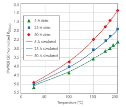
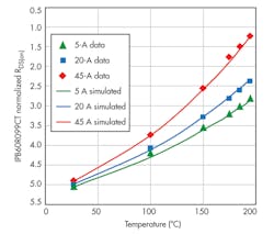
Figure 6 presents similar normalized measured data and simulated Rn curves for a second tested MOSFET IPB60R099 (600 V, 0.09 Ω at 25°C, and 18-A test current).
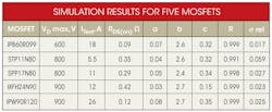
Other MOSFETs also were put through the same tests and simulations with the various sets of the coefficients a, b, c. The table provides the results, including the correlation factor R and sigma (relative).
Summary
After examining the dependence of RDS(on) change and related thermal coefficient K versus the maximum drain-voltage rating, the statistical analysis shows that MOSFETs with low Vd max are less dependable from a temperature perspective. The proposed solution is an enhanced empirical equation for simulation of the MOSFET drain-source resistance RDS(on) versus both the junction temperature and the drain current for the extended temperature range up to 200°C:

The proposed equation for simulation has been tested as well, with results and the relevant simulation coefficients provided for several MOSFETs with Vd maximum ratings covering the 600- to 900-V range.
References
1. Ralf Locher, “Introduction to Power MOSFETs and Their Applications,” Application Note AN-558, National Semiconductor, 1988.
2. IPB60R099 datasheet, Infineon.
3. Design Note AN9010, K.S. Oh, Fairchild Semiconductor, 2000.
4. “Using Simulation to Estimate MOSFET Junction Temperature in a Circuit Application,” David Divins, International Rectifier, 2007.
5. IPW90R120 datasheet, Infineon.
Alex Tyshko is a principal electrical engineer at PetroMar Technologies Inc. With 40 years of experience in power and high-temperature electronics, he previously worked for Halliburton ES and Spellman HV Electronics in the U.S. and in the satellite and other industries in Russia. He has an MSEE from Kiev Polytechnic Institute, Ukraine, and holds several patents.
About the Author
Alex Tyshko
Principal Electrical Engineer
Alex Tyshko is a principal electrical engineer at PetroMar Technologies Inc. With 40 years of experience in power and high-temperature electronics, he previously worked for Halliburton ES and Spellman HV Electronics in the U.S. and in the satellite and other industries in Russia. He has an MSEE from Kiev Polytechnic Institute, Ukraine, and holds several patents.
Comment About the Article
To join the conversation, and become an exclusive member of Electronic Design, create an account today!

Leaders relevant to this article: