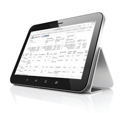
SEMI FabView offers interactive mobile fab forecast
San Jose, CA. SEMI has announced SEMI FabView, a mobile-friendly, interactive version of its World Fab Forecast quarterly report for electronic supply chain players and analysts. The new product was announced during the press conference at SEMICON Taiwan earlier this month, where 43,000 industry professionals convened. SEMI FabView tracks spending and capacities of over 1,100 facilities, including over 60 future facilities, across industry segments from analog, power, logic, MPU, memory, and foundry to MEMS and LED fabs.
SEMI FabView features high-level fab data such as capacity, technology nodes, and equipment spending, with other device manufacturing insights such as fabs by region, wafer size, product type, and construction status. This new online platform enables anytime access on the changes taking place in fab construction and expansion, production volume, device types, and more. The ability to quickly access the latest data for quarterly business reviews or earnings calls, or to validate an investment decision, is a key feature of this new product.
SEMI FabView users can
- view forecast for equipment and construction spending, capacity changes, and fab status from new plans to closures;
- organize data views by filtering data and accessing analyst commentary for each company and fab to see the latest SEMI forecast; and
- access forecast data by company, geographical region, wafer size, technology geometry and specific stages of fab life cycle—from announced and planned new fabs to fabs that are in transition (for example, when a cleanroom is converting to a larger wafer size or a different product type).
SEMI FabView is available for a product demo.
About the Author

Rick Nelson
Contributing Editor
Rick is currently Contributing Technical Editor. He was Executive Editor for EE in 2011-2018. Previously he served on several publications, including EDN and Vision Systems Design, and has received awards for signed editorials from the American Society of Business Publication Editors. He began as a design engineer at General Electric and Litton Industries and earned a BSEE degree from Penn State.

