Arm to Move Chip Design to Arm-Based Servers in AWS's Cloud
This ElectronicDesign article has been reprinted here with permission.
Arm, which designs the blueprints to central processing units and other chips used in smartphones and data centers, said it would use Amazon’s cloud computing service to run more of the software tools used by its engineers. Arm plans to move most of its electronic design automation work to AWS, the technology giant's cloud, to help it develop new chips faster and more cheaply.
Today, the most advanced computer chips contain billions of transistors that are around 100,000 times smaller than the width of a human hair. These tiny electronic switches are lashed together in millions of so-called logic gates that are, in turn, combined into thousands of other components like memory caches and accelerators for AI that are carefully packed in a constrained space on the die.
But modern microprocessors have become so intricate that it's impossible for engineers to design every single detail by hand. Instead, they use electronic design automation (EDA) software to streamline many steps in the process: from placing thousands of components on the floor plan of the chip to verifying the performance of the device and preparing it ahead of final production.
Building a central processing unit (CPU), system-on-a-chip (SoC) or other category of chip is a complicated three-dimensional design problem. The complete process can take many months to even several years. It also involves massive amounts of computing power and data storage, which Arm now plans to rent out through AWS instead of relying on its own in-house server infrastructure.
Arm last month announced it would move most of its EDA workloads, including production-level design validation, to AWS as part of the project with Amazon’s cloud computing subsidiary. For Arm, the advantage of the cloud is that Arm can scale its computing power and storage faster and more cheaply than buying servers and software for internal use, giving its engineers more flexibility and freedom to sort out problems with its chips.
According to Arm, running EDA workloads in the cloud at production scale is a semiconductor industry first, and the company believes it will lead the way for transformation of the segment.
Arm already uses AWS to run software that it uses to simulate and test the performance, power and other features of its microprocessors before the blueprints are rolled out to customers. It also uses machine learning tools from Databricks to crunch data from every step in the development process in Amazon's cloud and analyze it to pinpoint potential areas for improvement in its semiconductors.
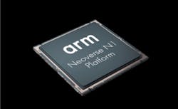
Arm is also tapping server chips with its intellectual property inside. Arm said that it would run workloads on clusters of compute power or instances powered by Graviton 2, a central processing chip designed by AWS based on Arm's Neoverse CPU cores. Arm said that it leverages the Graviton CPUs to bolster throughput for its engineering workloads, improving its throughput per dollar by over 40% compared to chips based on the x86 architecture, which both Intel and AMD use.
Rene Haas, who leads the intellectual property products group at Arm, said as part of the project, "we've focused on improving efficiencies and maximizing throughput to give precious time back to our engineers to focus on innovation." He said that thanks to AWS’s Graviton2 instances "we're optimizing engineering workflows, reducing costs, and accelerating project timelines to deliver powerful results to our customers more quickly and cost effectively than ever before."
According to Arm, it has managed to improve the performance of its EDA software by a factor of 6, while boosting throughput for other engineering jobs 10-fold, reducing cost and time-to-market.
Arm sells the blueprints to chips that are used in 90% of smartphones in the world, including Apple's A-series chips. The company is also investing in alternatives to Intel chips that dominate massive data centers and is rolling out power-sipping cores used in Internet of Things devices. Arm licenses its intellectual property (IP) to both technology giants and startups—over 500 customers in all—that have shipped more than 180 billion chips based on its instruction set architecture (ISA) to date.
Arm plans to move more of its development tools to Arm-based servers in the cloud in the future and it hopes to persuade customers in the semiconductor industry to follow in its footsteps. The company, which has its home base in Cambridge, England, and US headquarters in Silicon Valley, plans to cut its global data center footprint by at least 45% as it completes the shift to the cloud. The long-term strategy is to reduce its use of on-premise compute by 80%, Arm said.
The company has also partnered with top semiconductor software firms including Cadence Design Systems, Mentor Graphics and Synopsys to port their EDA tools to run on Arm-based hardware.
About the Author
James Morra
Senior Editor
James Morra is the senior editor for Electronic Design, covering the semiconductor industry and new technology trends, with a focus on power electronics and power management. He also reports on the business behind electrical engineering, including the electronics supply chain. He joined Electronic Design in 2015 and is based in Chicago, Illinois.
Voice Your Opinion!
To join the conversation, and become an exclusive member of Electronic Design, create an account today!

Leaders relevant to this article:

