Input Protection for Low-Distortion Op-Amp Circuits

Download this article in PDF format.
A subject rarely found in circuit design textbooks is the matter of nonlinear junction capacitance, especially reverse-bias junction capacitance, also called depletion capacitance. When it is discussed, it’s usually with regard to fast switching circuits, and even then, it’s normally treated as linear.
Yet in many situations, junction capacitance will be found to be the main cause of distortion in otherwise highly linear analog circuits. This article is principally concerned with two instances of this phenomenon, often encountered simultaneously: input protection circuits and common-mode distortion in op amps.
Junction Capacitance
We needn’t go very deeply into the physics of PN junctions, since we’re concerned here with how to make use of existing devices rather than how to design silicon wafers. Suffice it to say that the interface between P and N contains no net charge and is called the depletion region. Thus, it behaves like an insulator, sandwiched between the remaining conductive regions. We therefore have a diode, but also a capacitance.
The greater the reverse voltage applied across the diode junction, the wider the depletion region grows, effectively separating the capacitor’s “plates” further. Increasing reverse-bias causes shrinking junction capacitance, but the relationship isn’t a linear one. The junction capacitance can be estimated using:
C = Co/(1+V/Vb)x
where Co = capacitance with zero bias; V = applied reverse-bias voltage; Vb = built-in voltage, about 0.6 to 0.7 V; and x = Empirical constant <1.
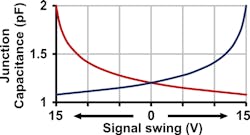
A value for Co is often quoted on diode datasheets, allowing for relative comparison between different devices. As a real-world example (Fig. 1) shows, the above formula fitted to actual measured data for a 1N4148—a commonly used signal diode—demonstrates useful agreement. The curve is, of course, unpleasantly nonlinear.

Junction Capacitance and Distortion
To appreciate the effect this can have on a linear circuit, consider Figure 2, which shows a simple network consisting of a series resistance and a pair of diodes, each reverse-biased to the bipolar power rails. Such a network often forms part of an overvoltage protection circuit. Any incoming voltage greater than the supply rails (plus one diode drop) will be clamped, protecting any downstream device. In practice, the resistor may be explicitly included to limit the fault current through the diodes, or it may be implicit within the source impedance of whatever the signal source is, or a mixture of both.
Figure 2 also shows the total harmonic distortion plus noise (THD+N) measured for this circuit using Audio Precision System 1, or AB1 (80-kHz measurement bandwidth), adjusted to achieve 20 dBu at the analyzer input. This is large enough to maintain a good signal-to-noise ratio for the analyzer, but still well below the conduction threshold of the diodes. The dotted trace indicates the measurement with the diodes removed, which is the measurement floor of the analyzer.

Adding a pair of 1N4148s reveals the scale of the problem: They introduce significantly more distortion, mainly odd harmonics (Fig. 3). The distortion declines above 10 kHz due to harmonics being filtered out by the input capacitance and bandwidth limit of the analyzer.

As a reality check that this is indeed caused by junction capacitance, consider Figure 4, which shows the 1N4148 capacitance curve from Figure 1 earlier, mirrored to represent the two diodes in the test circuit. They’re effectively in anti-parallel from the point of view of the signal, so the total will be the instantaneous sum of the two.
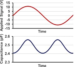
When applying the 20-dBu signal, the total capacitance varies as shown in Figure 5, from about 2.4 pF to almost 2.6 pF, twice every cycle (in reality, the diodes are unlikely to be perfectly matched, but that’s not important to the point being made). The variation itself is a distorted cosine with an RMS value of 56 fF.
At first, it might seem unlikely that a couple of picofarads varying by mere femtofarads would have any detectable effect in the audio band. After all, 56 fF has a reactance of 284 MΩ at 10 kHz, which is surely of no consequence? But a 20-dBu signal imposed across this reactance draws 27 nA of nonlinear current through the source impedance, causing a nonlinear error voltage to appear across it, which is effectively added to the audio signal. In this case, the source impedance is 10 kΩ, so the error voltage should amount to about 270 μV, which is −89 dB or 0.0035% THD. The actual measured value was 0.0038%. In other words, the ratio of the capacitive reactance to source impedance gives the level of distortion to be expected.
At least we’ve identified the problem, making it easier to identify a solution: either make the capacitance more linear or make it irrelevant. The former is nontrivial, but we can certainly substitute a different pair of diodes having much lower capacitance. The BAV99 is such a device, containing two diodes with similar specifications to the 1N4148 but less than half the advertised capacitance. As shown in Figure 2, they deliver a considerably better result.
Common-Mode Distortion
Having witnessed the influence of junction capacitance using discrete diodes, it becomes easier to appreciate the same effect taking place in op amps. Here, it’s called common-mode distortion because it occurs when an op amp is configured in non-inverting mode, meaning there’s a common-mode voltage on each input when amplifying a signal.
The distortion is caused by exactly the same mechanism of nonlinear junction capacitance considered previously, but this time within the op amp itself. It will be due principally to the base-collector capacitance of the internal input transistors, and to any parasitic diodes between the inputs and the substrate.
In inverting mode, there’s no voltage variation at the inputs and no additional distortion. In non-inverting mode, though, both inputs follow the signal voltage, leading to nonlinear modulation of the input capacitance. This has prompted a general engineering maxim of “always invert,” but that’s not always convenient. And if we need overvoltage protection, then we may be compounding the problem, as we shall see later. Before doing that, let’s first explore common-mode distortion in isolation.
The effect is well demonstrated with a TL07x FET-input op amp, as it has relatively large junction capacitances between the inputs and substrate.1,2 It’s also the sort of op amp used when a very large input impedance is needed cheaply, which implies a large source impedance—all of the ingredients for common-mode distortion.
Figure 6a shows a test circuit using one half of a TL072 arranged for a non-inverting gain of unity (but a noise gain of ×2). The same figure shows the measured distortion at 14 dBu in/out, which is indistinguishable from the measurement floor.
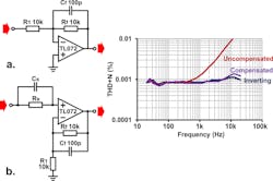
Figure 6b shows the circuit reconfigured for a non-inverting gain of ×2 (same noise gain). A bias-current path from the input node to ground isn’t shown but is assumed hereafter. The trace labeled “uncompensated” has the same 14-dBu input level and is considerably worsened. That’s due to the nonlinear capacitance of the inverting-input pin being modulated by the feedback signal, causing a nonlinear current to be drawn through the feedback path and therefore an error voltage across it. It was strongly dominated by the second harmonic since there’s only one junction this time, making the loading more asymmetric.
The non-inverting input pin is similarly modulated, but since the source impedance is extremely small (50 Ω for the Audio Precision), negligible error voltage is developed there. A fine example of common-mode distortion.
The foregoing description also hides within it the solution to the problem. Since the non-inverting input is also modulated, putting a suitably matched impedance in series with it will cause an identical error voltage to be developed there, too. These distortion errors, being common mode, will be rejected by the op amp, canceling out the (unfortunately named?) common-mode distortion.
The Thévenin source resistance seen by the inverting input is Rf and R1 in parallel, so the required compensating resistance is 5 kΩ, plus a parallel capacitor to match Cf. Forgetting to include the extra capacitor will achieve only partial cancellation, although the capacitors can be low-quality types without spoiling performance. The result is shown by the trace labeled “compensated,” which is barely worse than the measurement floor.
The price we pay for distortion compensation (apart from a few pennies in components) is Johnson noise. In this case, the audio-band EIN increased from −102.6 dBu with no compensation to −99.7 dBu with it. Modern alternative devices like the OPA164x offer an isolated substrate and negligible common-mode distortion, but they’re also a lot more expensive. It’s left to the designer to decide what’s more important.
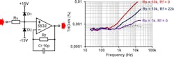
A unity-gain buffer is the worst culprit for common-mode distortion since it endures the largest common-mode signals at its input. Figure 7 shows the result using a bipolar op amp, the NE5532. With a 10-kΩ source resistance, the distortion is severely degraded, but adding a matching 10-kΩ feedback resistor eliminates this completely.
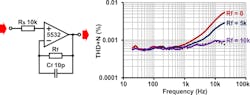
It’s a simple cure, but be aware that adding a resistance in the feedback loop will also introduce a pole that may reduce the phase margin and affect stability. Thus, some op amps may require a small capacitance in parallel with Rf. However, using a very small value (e.g., 10 pF in this case) should be sufficient to avoid the need for a matching capacitance across Rs.
Input Protection plus Common-Mode Distortion
Now, suppose we need an input buffer with overvoltage protection and we’re not free to use premium, low-capacitance devices, perhaps for reasons of cost. Figure 8 shows the previous circuit now with protection diodes to each rail—a textbook arrangement. The series resistance Rs is required in some form to limit the current through the diodes during overload. In reality, this might be an explicit series resistor, or it may be the implicit source impedance of an input attenuator, or whatever.
The distortion results are also shown in Figure 8. Here, we can see that even with a minimalist 1-kΩ source resistance, distortion is already noticeably worse than the measurement floor, because the diodes are now contributing additional junction capacitance distortion. If we need the fault-limiting resistance to be larger, say 10 kΩ, distortion becomes woeful, exceeding 0.01% at 20 kHz. Adding a matching resistance in the feedback loop can now only partially compensate for all of the distortion taking place at the non-inverting input node. Manual adjustment proved that 22 kΩ produced the best compensation, but even this is disappointing.
How can we improve on this design? One option is to move the protection diodes to the inverting input. In turn, a pair of antiparallel diodes also must be added between the two inputs to complete the fault current path from input to either rail. Since there’s normally no voltage difference between the op amp inputs, i.e. across these diodes, their junction capacitance remains constant. In other words, they’re bootstrapped.
In fact, the 5532 already has these diodes internally as shown in Figure 9 (when relying on internal diodes, the fault current should be limited to <5 mA to avoid fusing the internal bond wires3). With this arrangement, we have a similar situation to one previously: One op-amp input sees only common-mode distortion, but the other sees common-mode distortion plus protection diode distortion, so full distortion cancellation is again not possible.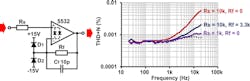
However, it does bring down the overall distortion levels and leads to a smaller compensation resistance, meaning less noise. In this case, a 3.3-kΩ feedback resistor gave optimum cancellation with a 10-kΩ source resistance. The reason for showing this circuit is for interest, because it’s the approach used in the Audio Precision S1 analyzer itself.
Better Overvoltage Protection
Can we do better still? And can we do it without needing a distortion meter to find the optimum cancellation resistance? The answer is yes.
Keen-eyed readers will already have spotted the clues laid in the previous paragraphs. The best approach is to maintain the same junction capacitances at both input pins and combine them with matching source impedances. This pretty much guarantees optimum distortion cancellation with no special tools required, and it’s independent of the op-amp type being used. Figure 10 shows the circuit.
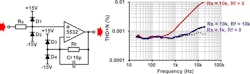
Putting Rf = Rs = 10 kΩ now produces the same result as a mere 1-kΩ source resistance alone. The remaining rise at high frequencies is mainly due to residual mismatching between the diode pairs. Even atrocious power diodes still yield quite good results this way.
Nevertheless, a final criticism that can be leveled at the previous circuit(s) is that the fault current is pumped into the rail(s), which may not be able to sink it. This can be corrected by returning the protection diodes to dedicated shunt references, e.g. a pair of Zener diodes. Fault current will then be directed safely to ground, and the Zeners can of course be chosen to suit the clamping requirements. It’s essential to bias the Zeners with some standing current, otherwise gross distortion will result. Fortunately, the standing current can be very small, less than 1 mA if necessary.
Figure 11 shows the improved circuit. When combined with low-capacitance diodes, ideally in a single package such as a BGX50A (a single package gives some hope of good matching between diode pairs), exemplary performance is achieved. As shown in the figure, with proper compensation, there’s no significant distortion within the audio band.

The circuits shown so far have used a 10-kΩ input resistor, which is representative of many real-world interfacing situations. If the Zener clamping option is used, then peak input overloads of several hundred volts can be handled this way, provided the Zeners and limiting resistance have sufficient power rating.
However, both the NE5532 and TL072 exhibit further HF distortion with source impedances much above 10 kΩ, even after compensation. Therefore, for very large source impedances, other op amps must be tried. For example, the OPA1662 and OPA1678 perform well with source impedances up to at least 100 kΩ.
An alternative means for limiting current without using a simple resistance is to employ a current-clamping circuit like that in Figure 12, built from depletion MOSFETs. Under signal conditions the MOSFETs short out their own body diodes and behave like a total resistance of about 3 kΩ, which is distortion compensated by Rf. If the voltage across the MOSFETs exceeds a couple of volts, they enter the saturation region and current is limited to the IDSS of less than 2 mA.4
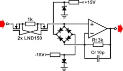
The reduced resistances minimize noise contribution while still allowing overloads up to 500 V dc to be tolerated. Of course, if the source impedance is variable, perhaps because it’s a switched attenuator or potentiometer, then either we must vary the compensation impedance in sympathy (as was done in the Audio Precision analyzer), or else use a compromise value and live with it.
Merlin Blencowe is Analog Design Engineer at AMS Neve Ltd.
References
1. Caldwell, J. (2014) “Distortion and source impedance in JFET-input op amps.” Texas Instruments Analog Applications Journal, Q4, pp. 4-6.
2. Gross, W. H. (1994) “Source Resistance Induced Distortion in Op Amps.” Linear Technology Design Notes, No 84.
3. Buxton, J. (1994) Simple Techniques Protect Amplifiers from Input Overvoltage. Analog Dialogue, Vol 28, No3, pp. 13-16.
4. Horowitz, P. & Hill, W. (2015). The Art of Electronics, 3rd ed. Iliffe & Sons Ltd., London, p. 362.
About the Author
Merlin Blencowe
Analog Design Engineer, AMS Neve Ltd.
Comment About the Article
To join the conversation, and become an exclusive member of Electronic Design, create an account today!

Leaders relevant to this article: