CTSD Precision ADCs (Part 3): Inherent Alias Rejection Made Possible
This article is part of the Analog Series: Optimizing Digital Processing with CTSD Precision ADCs
Members can download this article in PDF format.
What you'll learn:
- A look at the Nyquist sampling theorem.
- How to deal with aliasing by attenuating signals using low-pass filters (i.e., an antialiasing filter, or AAF).
- AAF requirements for different ADCs.
- A deep dive into the inherent alias-rejection property of a CTSD modulator loop.
Part 1 of this series showcased a new class of easy-to-use, alias-free precision ADCs based on continuous-time sigma-delta (CTSD) architecture that offers simple, compact signal-chain solutions. Part 2 demystified the CTSD technology for signal-chain designers.
In Part 3, we compare the design complexity behind alias-rejection solutions for currently available precision ADC architectures. The article illustrates a theory to explain the inherent alias rejection of the CTSD ADC architecture. It also showcases how signal-chain design can be simplified and discusses the extended advantages of CTSD ADCs. Furthermore, it introduces new measurement and performance parameters to quantify alias rejection.
In many applications like sonar arrays, accelerometers, vibration analysis, etc., signals outside the signal bandwidth of interest are observed, referred to as “interferers.” The key challenge for signal-chain designers is that the ADC sampling phenomenon causes these interferers to alias into the signal bandwidth of interest (in-band) and degrade performance. Apart from this, in applications like sonar, interferers aliasing in-band could be misinterpreted as an input signal, causing misdetection of objects around the sonars.
Solutions to reject these aliases are one of the reasons why traditional ADC signal-chain designs are quite complex. The unique inherent alias-rejection property of CTSD ADCs provides a new simplified solution. Before we delve into this groundbreaking solution, one should have a good understanding of the concept of aliasing.
Revisiting the Nyquist Sampling Theorem
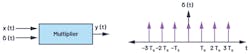
To understand the concept of aliasing, let’s quickly review the Nyquist sampling theorem. One could analyze a signal in either the time domain or frequency domain. In the time domain, the sampling of an analog signal is represented mathematically as multiplication of the signal—for example, x(t) with an impulse train, δ(t), having time period Ts (Fig. 1).
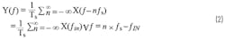
Equivalently in the frequency domain, the sampled output can be expressed using a Fourier series as:

Equation 1 simply means that if the frequency axis is unfurled, images of the input signal are formed at every integer multiple of sampling frequency fs.
Equation 2 indicates that the signal content of X(f) at frequencies f = n × fs - fIN, where n = 0, ±1, ±2, … …, will manifest itself at fIN after sampling, similar to the undersampling scenario in Figure 2, which illustrates the sampling phenomenon under various conditions.
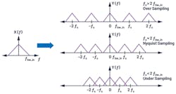
In summary, the Nyquist theorem states that any signal greater than half the sampling frequency folds or mirror backs to frequency less than fs/2. Thus, it can potentially fall into the frequency band of interest.
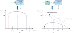
Assume an ADC is sampling at frequency fs and there are two out-of-band tones/interferers in the system—f1 and f2 at the ADC input as shown in Figure 3. Applying the Nyquist theorem, we can infer that since the frequency of tone f1 is less than fs/2, after sampling, its frequency remains the same. While the frequency of tone f2 is greater than fs/2, it will alias itself in the frequency band of interest, fbw_in, and degrade the performance of the ADC in this region (Fig. 3a).
This theory also can be extended to any noise beyond fs/2. Such noise folds back and manifests itself in-band as well, increasing the in-band noise floor and degrading performance.
An Incumbent Solution for Aliasing
A simple solution to avoid this performance degradation due to out-of-band (OOB) tone or noise foldback is to attenuate any signal content beyond fs/2 before being sampled by the ADC using a low-pass filter, which is known as an antialiasing filter (AAF). Figure 3b shows the transfer function of a simple AAF and illustrates the attenuation-to-alias tone at frequency f2 before it folds back in-band.
The main characteristics of that AAF would be the order of the filter and –3-dB corner frequency. They are determined by passband flatness, the absolute attenuation required at certain frequencies (like sampling frequency), and the slope of attenuation required beyond input bandwidth (also called transition band). A few common filter architectures are Butterworth, Chebyshev, Bessel, and Sallen-Key, which can be implemented using passive RC and op amps. Filter design tools are available to assist signal-chain designers with AAF design for given architecture and requirements.
Let’s look an example application to understand the antialiasing filter requirements. In a submarine system, the sonar sensor emits sound waves and analyzes the echoes underwater to estimate the position and distance of surrounding objects. The sensor has an input bandwidth of 100 kHz and the system detects any tone of magnitude > –85 dB at the ADC input as a valid source of echo. Therefore, any interference from out-of-band would need to be attenuated by at least –85 dB by an ADC to avoid detection as input by the sonar system. For these requirements, the next section will explore building the alias-rejection solutions for different ADC architectures and then compare them.
In traditional ADC architectures, such as successive-approximation-register (SAR) and discrete-time sigma-delta (DTSD) ADCs, the sampling circuit is at the analog input of the ADC, indicating that an AAF is required before the ADC input (Fig. 3b, again).
AAF Requirements for SAR/Nyquist Sampling ADCs
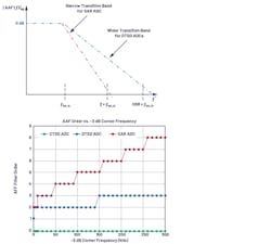
SAR ADCs generally have a sampling frequency set to two or four times the analog input frequency (fIN). The AAF for such an ADC would need to have a narrow transition band beyond frequency fIN, implying a very high order filter is required.
From Figure 4, we can see that a SAR ADC with a sampling frequency of approximately 1 MHz requires a fifth-order Butterworth filter to get –85 dB rejection for frequencies greater than 100 kHz. In terms of filter implementation, as the order of filter increases, so too does the number of required passives and op amps. This means an AAF for SAR ADCs requires a significant amount of power and area budget in signal-chain design.
AAF Requirements for DTSD ADCs
Sigma-delta ADCs are oversampled ADCs, meaning sampling is much higher than the analog input frequency. And the region of aliasing to be considered for AAF design is fs ± fIN. The transition band requirement for the filter would be from fIN to very high fs. This is a wider transition band when compared with a SAR ADC AAF, showing that the order of AAF required is also lower. Figure 4 shows that to get –85-dB rejection for frequencies around fs to 100 kHz for a 6-MHz sampling frequency DTSD ADC, a second-order AAF is generally required.
In a practical scenario, interferers or noise could be anywhere in the frequency band and not restricted to being around sampling frequency fs. Any frequency tone less than fs/2, like the tone at frequency f1 in Figure 3, wouldn’t manifest into in-band to degrade the ADC performance. Though the AAF may attenuate the tone f1 to a certain extent, it’s still present in the ADC output and is unnecessary information that must be processed by the external digital controller.
Could this tone be further attenuated so that it’s not seen at the ADC output? One solution could be to use an AAF with a narrow transition band beyond frequency fIN. However, this would increase the filter’s design complexity. Alternative solutions are on-chip digital filters that are part of sigma-delta modulator loops.
Digital Filters of Sigma-Delta Modulator Loops
In sigma-delta ADCs, because of oversampling and noise shaping, the modulator output contains lots of redundant information and thus requires a large amount of processing by the external digital controller. This redundant information processing can be avoided if modulator data is averaged, filtered, and provided at a lower output data rate (ODR), which is generally 2 × fIN. Decimation filters are used to convert the sampling rate from fs to the required lower ODR.
Sample-rate conversion using a digital filter will be explained in future articles, but the key point here is that a discrete-time sigma-delta modulator is usually partnered with an on-chip digital filter. Figure 5 shows the combined signal transfer function (TF) for interferers with the analog filter in front and digital filter on the back end of a modulator.
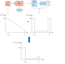
In conclusion, the AAF for a DTSD ADC is designed based on the attenuation required for tones around alias region fs. And the tones in a non-aliasing region like f1 are completely attenuated by the on-chip digital filters.
Back-End Digital Filter vs. Front-End Analog Filter
A SAR ADC requires a narrow transition band in an AAF, while a sigma-delta ADC requires a narrow transition band in a digital filter. Digital filters are low power and easy to integrate on-chip. Also, programming the order, bandwidth, and transition band of a digital filter is much simpler than with an analog filter.
Oversampling is advantageous in that it allows for the use of a wide transition analog filter combined with a narrow transition digital filter on the back end. This provides an optimized solution in terms of power, space, and immunity to interferers.
With the use of DTSD ADCs, the AAF requirements, though relaxed, add design complexity to meet settling-time requirements after every sampling event to avoid performance degradation of a signal chain. The challenge for signal-chain designers is to fine-tune the AAF to balance between alias-rejection and output-settling requirements.
The new class of precision CTSD ADCs simplifies the signal-chain design by eliminating the need for front-end analog filter design.
The Inherent Alias Rejection of CTSD ADCs
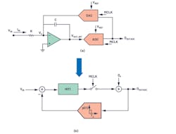
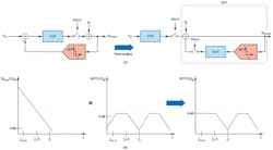
In Part 2 of this series, a first-order CTSD modulator was built from a closed-loop resistive inverting amplifier (Fig. 6). A CTSD modulator follows the same concept of oversampling and noise shaping as a DTSD modulator counterpart to achieve the desired performance. It has a resistive input rather than a switched capacitor input. The modulator building blocks include a continuous-time integrator, followed by a quantizer that samples and digitizes the integrator output and a feedback DAC that closes the loop at the input. Any noise at the input of a quantizer is shaped by the integrator’s gain transfer function.
Expanding on the information from Part 2, a simplified block representation for a CTSD modulator loop can be drawn with the following mathematical models:
- The integrator transfer function, generalized as H(f), is also known as a loop filter. For a first-order integrator, H(f) = 1/2πRC.
- The functionality of the ADC is sampling and quantization. So, a simplified ADC model for analysis uses a sampler followed by an additive quantization noise source.
- The DAC is a block that multiplies in the input in the present clock cycle with a constant. Thus, it’s a block with an impulse response that’s constant during the sampling clock period and 0 the rest of the time.
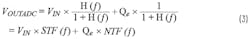
The equivalent block diagram with these simplified models (Fig. 6b) is widely used for sigma-delta performance analysis. The transfer function from VIN to VOUT is called signal TF (STF) and the Qe to output is termed as noise TF (NTF).
One reasonable explanation about the inherent alias-rejection property of a CTSD modulator loop would be that sampling occurs not directly at the input of the modulator, but after the loop filter, H(f) (Fig. 6a). But to get a complete picture, a linear model without a sampler would be used to understand the concepts and the analysis would be extended to loop with the sampler.
Step 1: STF and NTF Analysis Using a Linear Model
Ignoring the sampler for analysis simplification, the linear model would be as shown in Figure 7.
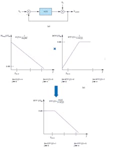
The STF and NTF for this loop can be represented as:
From Equation 3, the STF can be rewritten as:

Because the frequency bandwidth of interest is low frequency, mathematically it can be represented as f→0, while high frequency can be represented as f→∞. The magnitude of STF and NTF in dB as a function of frequency when plotted would be like that shown in Figure 7.
The NTF resembles a high-pass filter and the STF resembles a low-pass filter with flat 0-dB magnitude for the frequency band of interest and attenuation for higher frequencies that’s equivalent to AAF TF. Mathematically, the signal passes through H(f), which has a high-gain, low-pass filter profile and then is processed by the NTF loop. Now this understanding can be extended to loop with the sampler by first understanding the NTF block representation.
Step 2: Block Diagram Representation for NTF
With input VIN set to 0 V, the block diagram of the modulator loop can be rearranged as shown in Figure 8a and used for NTF representation. With the sampler in the loop, the NTF response would be similar to a linear model, but with replicated images at every multiple of fs (Fig. 8b).
Step 3: Rearranging the Modulator Loop to Visualize Upfront Filtering Action
If the loop filter H(f) and sampler of the modulator loop are moved to the input and feedback (Fig. 9), there’s no change with regard to the transfer function from input to output. The right side of this rearranged block diagram represents the NTF.
Similar to the linear model from Step 1, in the sampled equivalent system, the input signal traverses through high gain H(f), and then is sampled and processed through the NTF loop. The transversal of a signal through a loop filter creates a low-pass filter profile before it’s sampled. This profile leads to the inherent alias rejection of a CTSD modulator. Thus, the STF for a CTSD modulator loop is as shown in Figure 9.
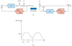
Step 4: Complete STF with a Digital Filter
To reduce the redundant high-frequency information, the CTSD modulator is partnered with on-chip digital decimation filters. Figure 10 shows the combined alias rejection TF. Alias from around fs is attenuated by the inherent alias-rejection property of a CTSD, while intermediate interferers are attenuated by a digital filter.
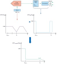
Figure 4 compares the order of AAFs required for SAR ADCs, DTSD ADCs, and CTSD ADCs for –80-dB rejection at the sampling frequency vs. the input signal bandwidth. The order and, hence, complexity of AAFs with SAR ADCs is the highest, while CTSD ADCs don’t require an external AAF as alias rejection is inherent to their design.
The Signal-Chain Advantages Made Possible by a CTSD Architecture
In certain multichannel applications like sonar beamforming and vibration analysis, the phase information between channels is important. For example, the phases between channels need to be accurately matched with a requirement of 0.05 degrees at 20 kHz.
For traditional ADC signal chains, the AAFs are designed using passive RC and op amps. The filter causes a certain magnitude and phase droop in-band that would be a function of corner frequency. For good channel-to-channel phase matching, all channels must have the same droop, which indicates the corner frequency of the filters for each channel need to be finely controlled and matched.
A second-order Butterworth filter designed for –80-dB rejection at 16 MHz (sampling frequency) and f3dB of 160 kHz (input bandwidth) could have a phase mismatch of ±0.15 degrees at 20 kHz with error tolerance of as low as 1% on the absolute values of RC. The availability of lesser-error-tolerance RC passives is limited and increases the bill of materials (BOM).
Since the AAF is eliminated in a CTSD ADC signal chain, the channel-to-channel magnitude and phase matching is inherently achieved in the frequency band of interest. The phase mismatch is limited by on-chip mismatches of analog modulator loop design, which could be as low as ±0.02 degrees at 20 kHz.
Measuring and Quantifying the Inherent Alias Rejection
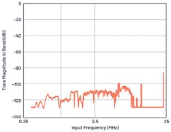
New functional checks to measure the alias rejection are introduced in the AD4134 ADC’s datasheet; it’s a precision ADC based on the CTSD ADC architecture. The frequency of the analog input signal of the ADC is swept. The impact of each out-of-band input signal is calculated by measuring the magnitude of tone folded back, if any, for the test frequency, with respect to the magnitude of the applied tone.
Figure 11 shows the alias rejection of the AD4134 for out-of-band frequencies in the performance bandwidth of 160 kHz with a sampling frequency of 24 MHz. For a frequency of 23.84 MHz (fs – 160 kHz), alias rejection is –85 dB, which is the alias rejection specification of the ADC. It also can be observed that the rejection is better than –100 dB for other intermediate frequencies. Further details on inherent alias rejection with options to further increase this rejection can be found in the AD4134 datasheet.
The CTSD ADC concepts explained so far can help signal-chain designers envision the unique properties of the resistive input, resistive reference, and inherent alias rejection of this architecture. An easy-to-drive input and reference coupled with the elimination of AAF design for CTSD ADC signal chains has led to a new simplified ADC front-end design for various applications.
Acknowledgements
The authors would like to thank silicon evaluation engineer Sanjay Kuna and senior test development engineer Richard Escoto for their efforts in testing and proving inherent alias rejection.
Read more articles in the Analog Series: Optimizing Digital Processing with CTSD Precision ADCs
References
Antialiasing Filter Design Tool Filter Design Tutorial
Kawle, Abhilasha and Wasim Shaikh. “CTSD Precision ADCs—Part 1: How to Improve Your Precision ADC Signal Chain Design Time.” Analog Dialogue, Vol. 55, No. 1, February 2021.
Kawle, Abhilasha. “CTSD Precision ADCs—Part 2: CTSD Architecture Explained for Signal Chain Designers.” Analog Dialogue, Vol. 55, No. 1, March 2021.
Kester, Walt. “MT-002: What the Nyquist Criterion Means to Your Sampled Data System Design.” Analog Devices, Inc., 2009.
About the Author
Abhilasha Kawle
Senior Analog Design Engineer, Analog Devices
Abhilasha Kawle is a senior analog design engineer at Analog Devices in the Linear and Precision Technology Group based in Bangalore, India. She graduated in 2007 from Indian Institute of Science, Bangalore, with a master’s degree in electronic design and technology.
Comment About the Article
To join the conversation, and become an exclusive member of Electronic Design, create an account today!

Leaders relevant to this article: