CTSD Precision ADCs (Part 5): Digital-Data-Interface Simplification with ASRC
This article is part of the Analog Series: Optimizing Digital Processing with CTSD Precision ADCs
Members can download this article in PDF format.
What you'll learn:
- Requirements for different types of sample rates.
- Conversion techniques for these different sample rates.
- Synchronous and asynchronous sample-rate conversion.
Digital-data-output sample rate is a key parameter of an analog-to-digital converter (ADC) signal chain for any application. However, varied requirements on the sample rate are different for each application. This article introduces a novel on-chip sample-rate conversion technique used on a core ADC’s output, allowing signal-chain designers to process the ADC digital output data at the desired sample rate for their application.
The job of an ADC is to sample the analog input signal and convert it into an equivalent digitized format. The sample rate at which an application requires the digital data for further processing needn’t be the sample rate at which the ADC samples the analog signal. Each application requires a unique digital-output sample rate. A sample-rate converter maps the ADC data at the input sample rate to the desired output sample rate.
This article starts with an overview of sample-rate requirements in various applications and establishes the need for an ADC to support a wide range of output sample rates. We follow up with a quick recap of traditional sample-rate conversion techniques in known ADC architectures and their shortcomings.
Next, we introduce the novel asynchronous sample-rate conversion (ASRC), which can be paired with any ADC architecture to get any desired output sample rate and simplify the digital interface design with the external digital host. Pairing ASRC with a continuous-time delta-sigma (CTSD) ADC offers the best of both worlds, simplifying the signal-chain design not only on the analog input side, but also on the digital output side of the ADC.
Sample-Rate Requirements
One of the major performance parameters for any ADC application that drives digital-data sample-rate selection is the accuracy expected from the ADC. The greater the number of samples in the digital data, the more accurate the representation of the analog input. But this would mean processing large amounts of data with its own penalty in external digital-host-interface design complexity and power.
So, based on the accuracy required, the budget for power and design complexity, and the algorithm processing planned, each application decides the sample rate of the digital data. Most of the general sample rates required can be categorized into the following:
Nyquist Sample Rate
The well-known Nyquist sampling1 theorem states that the sample rate should be at least twice the input bandwidth for faithful digital representation of the analog input. Therefore, Nyquist sample-rate applications have the digital sample rate at twice the input bandwidth of interest.
A well-known example for such a sample rate is digital audio data storage on a CD, which is at 44.1 ksamples/s, where the input audio bandwidth of interest reaches up to 20 kHz. This is the upper frequency limit of human hearing.
Oversample Rate
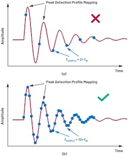
In a few applications, such as frequency-harmonic analysis or time-domain analysis, the sampling rate required would be multiple times higher than the input bandwidth. One example of an oversample rate is the time-domain analysis of a transient signal in a shock-detection environment (Fig. 1). If the sample rate for such a signal is the Nyquist sample rate, we will not get the complete picture of the peaks and turfs. Having more sample points results in faithful reconstruction and analysis of the signal.
Variable Sample Rate
In certain applications, such as coherent sampling, the requirement is to adjust the output sample rate based on the analog input frequency with good resolution. Power-line monitoring is one such example application that requires coherent sampling to meet the Class A power quality meters specified in IEC 61000-4-30.
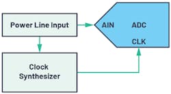
The accuracy requirements in such standards dictate that the sample rate needs to track the input-line frequency drift. In these applications, clock synthesizer circuitry on the power line generates the ADC’s output digital-data sample clock (Fig. 2).
Multisample Rate
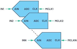
In multichannel applications that detect and analyze a wide range and different types of analog inputs, such as oscilloscopes or data acquisition, the sample rate can be different for each channel (Fig. 3). In this case, the ADCs used in the platform should have the flexibility to support a multisample rate.
Thus, we see that the digital-data sample-rate requirement is unique to the application, and there’s no one-size-fits-all sample rate. Hence, a broad market ADC would need to support a wide range of programmable digital-data sample rates.
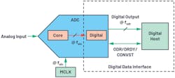
Figure 4 showcases a generalized ADC digital-data interface with the external digital host. Note: The digital-data interface discussed in this article doesn’t include the device configuration control interfaces such as SPI or I2C.
The core ADC samples the analog input with a sampling clock at rate fsin (Fig. 4, again). The input sampling clock itself is generally represented as MCLK in most datasheets. The final digital output data is at sample rate fodr. Usually, those pins are labeled as ODR or DRDY or CONVST clock in the datasheets. Here, we will use the blanket term ODR clock to represent the digital-output-data clock.
The ADC core’s sample rate (fsin) depends on the ADC architecture. The digital-output-data rate (fodr) depends on the data-interface requirements with the external digital host. In most ADC signal-chain applications, fsin and fodr can have different values and be uncorrelated. Hence, there’s a need for a sample-rate conversion that maps the ADC core’s data at fsin to the digital output data at fodr.
In the following sections, we will discuss traditional sample-rate conversion techniques used in well-known ADC architectures, such as Nyquist ADCs and oversampled ADCs. Also, we will offer insights into other associated digital-data-interface requirements.
Sample-Rate Conversion in Nyquist-Rate ADCs
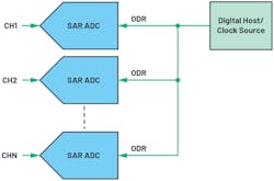
In Nyquist-rate converters, the ADC core’s sampling frequency is twice the analog input bandwidth (fin). The most common example under this category is the Nyquist-rate SAR ADC, where the input and output sample rates are the same. Thus, the digital output data rate clock (ODR) can be reused as the ADC core sample clock (MCLK).
In SAR ADC datasheets, the digital-output-data clock is represented as CONVST or DRDY. But, as indicated earlier, we will refer to all of these as ODR clock. The ODR and MCLK combination leads to a simplified digital data interface (Fig. 5) with only one clock routing. Since the clock is sourced and controlled either by an external clock source or an external digital host, the ADC is externally clocked. This means the ADC is running in an external hosted mode.
It’s easy to scale the sample rate fodr based on the application requirements and the analog input bandwidth. With fodr scaling, we’re also scaling the ADC core’s sample clock rate (fsin). An added advantage is that as fodr scales, the power of the entire ADC scales linearly. This simplified digital data interface leads to many other extended benefits, one of them being ease of synchronization in multichannel applications.
Ease of Synchronization
In a single-channel ADC application, the local clock provided to the ADC would synchronize the digital data inherently to the given clock. In multichannel ADC applications, the challenge is to guarantee synchronous sampling of multiple analog inputs and synchronization of digital data to the clock edge of the ODR clock for further digital processing.
There are many well-known examples of synchronized multichannel applications, such as an audio application where the left and right channels have specific synchronization requirements. Another typical example is monitoring various power lines in a power grid. Again, within each power line, synchronization is required between voltage, current, and power input measurements.
With Nyquist rate ADCs (Fig. 6), multichannel synchronization can be easily achieved by sharing and having well-planned routing of the ODR clock. Well-planned routing involves ensuring that the ODR clock propagates with equal delay to each of the ADCs and provides the best possible channel synchronization.
A simplified digital data interface is a significant advantage of Nyquist-rate converters. Let’s discuss a few digital-data-interface challenges where it falls short.
Limitations of Nyquist-Rate Control
Noise Scaling
In Nyquist-rate converters based on the analog input bandwidth of the application, the digital-data clock can be easily scaled. The clock scaling offers an advantage in power, but the ADC noise increases due to a phenomenon called alias foldback. The extension of the Nyquist sampling theorem is that any information beyond the Nyquist frequency folds back or aliases back into the frequency band of interest.
The ADC’s analog input would have a lot of unwanted information or noise from the source and the input analog circuitry, extending to very high frequency. The ADC sampling causes any input noise beyond fsin/2 to fold back, causing the noise in the input bandwidth of interest to increase. As seen in Figure 7, as the sampling rate reduces, more such external noise folds back, increasing the noise in the ADC’s output.
Clock Timing Constraints
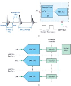
For SAR ADCs, the analog input sampling clock requires two phases (Fig. 9a). One is the sampling phase, where the input sampling capacitors of the ADC charge to analog input, and the other is the conversion phase, where this sampled data is digitized. The sampling circuits of the ADC generally require some minimum sampling time for the best possible ADC performance. Therefore, the external digital host or clock source generating this clock needs to adhere to these timing constraints.
Clock Jitter
A clock routing on an application board is sensitive to the supply noise of the clock source or coupling to other signals on the board, as this noise adds uncertainty to the clock edges. The uncertainty in the clock edges is known as jitter.
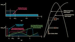
Various types of clock jitter on the sample clock can affect the ADC’s performance. The most common one is cycle-to-cycle rms jitter. It adds variability to the sampling point of the analog signal, resulting in performance degradation (Fig. 8). More details on how rms clock jitter affects ADC performance are explained in various articles.2
To summarize, the added error in the ADC data because of clock jitter can be quantified as degradation in signal-to-noise ratio (SNR):
where σj is the rms jitter.
Equation 1 implies that to meet the required SNRj, we either limit the input bandwidth or employ extra techniques to filter clock noise when the digital host or clock source is noisy.
Clock jitter is a more significant challenge in multichannel applications, where balancing synchronization and jitter addition due to long clock routings requires good clock architecture planning.3 Appropriate isolation and buffering are planned to ensure a low-noise clock at the ADC in such scenarios. Isolation is implemented using commonly available digital isolators, but it requires an extra budget in design complexity and power.
Now let’s next look into the sample-rate control technique used in oversampled ADCs.
Sample-Rate Conversion in Oversampled ADCs
As illustrated in earlier articles of this series, sampling and digitizing a continuous-time signal causes loss of information and introduces quantization noise in the sampled output. A class of ADCs follows the principle that the greater the number of samples, the better the accuracy and the lesser the quantization noise error. Hence, the analog input sample rate is higher than the Nyquist sampling rate and is termed oversampling.
Some new precision SAR ADCs use this technique of oversampling—they’re referred to as oversampled SAR ADCs. Figure 10a shows the noise advantage of oversampling SAR ADCs.
Another class of ADCs that uses the oversampling concept is the sigma-delta ADC.4 Here the quantization noise (Qe) is further shaped and pushed out to improve performance in the input bandwidth of interest. Figure 10b shows the noise-shaping characteristic of quantization noise for a sigma-delta modulator. Mathematically, the sampling frequency is OSR × fodr/2, where OSR is the oversampling ratio.
Directly interfacing the core ADC’s oversampled data to the external digital host implies overloading it with a lot of redundant information. Moreover, in some cases, the host may not support the stringent timing constraints required for such a high digital-data-rate transmission, and it could cause high power dissipation.
Consequently, it would be optimal if only the performance-optimized data in the input bandwidth of interest is provided. This would mean the output digital data rate should be reduced or decimated to the Nyquist rate (2 × fin), or a few multiples of the Nyquist rate, as desired by the application. Hence, a sample-rate converter is needed to map the ADC’s core data at a high sample rate of fsin to the required fodr.
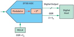
Traditionally, a digital sample-rate conversion technique called decimation is available—it filters and decimates the core ADC data by multiple 2N (Fig. 11). An input sampling clock (MCLK) is delivered to the ADC. The desired digital-output-data sample-rate (ODR/DRDY) clock, which is a divided version of MCLK, is provided as output. The division ratio is achieved by programming N, based on the required decimation rate.
To get a much finer resolution on fodr programming, the MCLK also can be scaled based on the input bandwidth requirement of the application. If we observe the digital data interface of oversampled ADCs, the ODR clock is given and controlled by the ADC. This means the ADC provides the clock, which is named the ADC in host mode.
Thus, with decimation as a sample-rate conversion technique, the ADC can provide high-performance digital data at a lower output data rate. But this technique has its own limitations.
Limitations of Decimation as Sample-Rate Control
Nonlinear Noise, Power Scaling
In variable-rate applications, the decimation rate, the MCLK, or both can be scaled. When only the decimation rate is increased, it reduces fodr and decreases noise as the digital filter filters more quantization noise. Only the power in the digital filter decreases linearly. If MCLK is reduced as discussed in SAR ADCs, the power of the entire ADC decreases linearly, but noise increases due to alias foldback.
Many systems adjust both the ADC’s MCLK and decimation rate to achieve a wide range of ODR. However, this approach can result in an undesired step change in measurement noise performance or system power performance.
Clock Jitter
Since the input sampling clock frequency (fsin) is higher with oversampled ADCs, they’re much more sensitive to clock jitter than the Nyquist-rate SAR ADCs, as indicated by Equation 1. Therefore, the clock source and the clock routing for an MCLK are planned based on jitter noise tolerable by the application. Be it a single-channel or multichannel application signal chain, many switching signals would be running across the application board.
Coupling from such noisy signals can increase the clock jitter on an MCLK. Thus, isolation must be planned for an MCLK using digital isolators for optimum ADC performance. This extra design planning pays a price in area and power. As indicated earlier, for finer resolution in fodr programming, an MCLK also is scaled. However, the availability of an MCLK clock source with the required fsin value and jitter requirements may be limited.
Synchronization
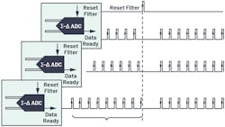
Achieving synchronization is another added challenge in oversampled ADCs. Generally, an extra pin called SYNC_IN is provided for synchronization in sigma-delta ADCs. The trigger of the SYNC_IN pin initiates simultaneous sampling of analog input and reset of decimation filters. After the digital-filter settling time, the digital output data is synchronized. The digital output data during the settling of the digital filter is interrupted (Fig. 12).
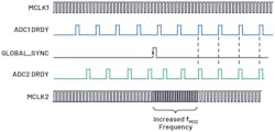
It also assumes that the MCLK and SYNC_IN command of all ADCs is synchronized. Achieving such synchronization on a high sample-rate clock, especially in the presence of isolators or synthesizers, would be a big challenge. One system solution identified toward solving the data interruption and synchronization challenge is a clock-synthesizer circuit, such as a phase-locked loop (PLL), which would generate synchronized MCLKs for all of the channels (Fig. 13).
To quickly summarize, when the SYNC_IN pin is triggered, the PLL initiates the clock synchronization to a reference clock. During the time the PLL settles, the MCLK rate adjusts such that at the end of it, the input ADC sampling edge and the ODR clock edges are synchronized. The how’s and what’s of this solution can be found in “Newest Sigma-Delta ADC Architecture Averts Disrupted Data Flow When Synchronizing Critical Distributed Systems.”5
The takeaway is that, with extra on-board circuit, PLL, or clock-synthesizer requirements when compared to SAR ADCs, the synchronization of sigma-delta ADCs or oversampled SAR ADCs adds to design complexity and power. ADI has explored another novel technique that helps ease the challenge of synchronization to a certain extent, called synchronous sample-rate conversion.
Synchronous Sample-Rate Conversion
A solution to a few of the discussed challenges of simple decimation is using a synchronous sample-rate conversion (SRC).6 The advantage of SRC is that the decimation rate can be any integer or fractional ratio of fsin, allowing for granular control of fodr. ADI has explored this technique and paired it with a precision discrete-time sigma-delta (DTSD) converter in the AD7770. More details on SRC can be found in the datasheet or reference material of the AD7770.
The highlight is that, with the possibility of fine resolution in fodr programming in SRC, synchronization becomes easier. For example, instead of tuning the external MCLK, the decimation rate is varied in very fine steps. So, when SYNC_IN is triggered, the channels would be synchronized (Fig. 14).
Achieving finer fodr without scaling the MCLK is an answer to most of the limitations discussed with the simple decimation technique. SRC also has its own limitations and challenges to solve.
Limitations of SRC
The synchronization challenge of having the same MCLK for all channels isn’t addressed with SRC.
Clock Jitter/Synchronization
SRC has the same limitations as a simple decimation sample-rate control in terms of MCLK jitter. The sensitivity of ADC performance to clock jitter because of high fsin must be addressed by planning isolation-barrier or noise-filtering circuits on the MCLK. This challenge further scales up in multichannel applications owing to the routing of the MCLK to multiple ADC channels.
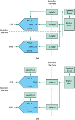
To achieve synchronization, the MCLK and SYNC_IN pin signals must be synchronized (see Fig. 16a below). The challenge is that all clocks reach the ADCs at the same time, independent of the PCB distance from the clock and the possible delays through the isolation barrier. A carefully designed clock plan, including the isolation barrier and the routing architecture, needs to be built to ensure that all ADC channels equally see delays, even with isolators in the path.
Interface Mode
The digital data interfaces we’ve discussed so far are the host mode and the hosted mode, and there’s a correlation to the ADC core architecture. For example, Nyquist-rate ADCs’ digital data clock is controlled and provided by an external clock source or digital host. Hence, they’re limited to be programmed as hosted mode. Oversampled ADCs provide and control the digital clock to the external digital host. Therefore, they’re limited to be programmed as host mode. Thus, a general limitation exists in all sample-rate control techniques discussed to this point: The data interface can’t be independently planned.
A solution to most digital data interface challenges would be to decouple the MCLK clock and ODR clock domains. Therefore, ADI reintroduces the novel asynchronous sample-rate conversion (ASRC) technique. It enables the independence of the ODR clock and the data-interface clock—thus breaking the age-old barrier of ADC core architecture limiting the selection and control of the ODR clock.
Asynchronous Sample-Rate Conversion
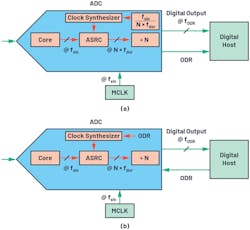
ASRC resamples the core ADC data at fsin in the digital domain and maps it to any desired output data rate. ASRC can be thought of as a digital filter that can achieve any noninteger decimation. However, an optimized implementation in terms of performance, area, and power would be one in which the ASRC handled the fractional decimation and was followed by a simple decimation filter to address integer decimation (Fig. 15). The ASRC resamples the ADC core data and decimates the data by fsin/N × fodr. The data at the output of ASRC is at the rate of N × fodr. At the same time, decimation filters get the required ÷N decimation.
In one form of ASRC implementation, the factor fsin/N × fodr can be programmed by the signal-chain designer. It would be based on the fsin of the ADC and the required fodr and N known from decimation filters implemented on the ADC. This is similar to programming the decimation rate in SRC—the difference being the decimation ratio can be an irrational ratio and a very fine resolution is possible. In this case, like in SRC, the ODR clock is synchronized to the MCLK and is an output generated on-chip by dividing the MCLK.
Another form of ASRC implementation is where the ODR clock is provided by an external clock source or digital host similar to Nyquist-rate converters. In this case, ASRC has an internal clock synthesizer that will calculate the fsin/N × fodr ratio and generate the required clocks for ASRC and decimation filters. The ODR needn’t be synchronized to MCLK and can be independently set at any sample rate.
Thus, in any form, the ASRC technique enables signal-chain designers to granularly set fodr and go beyond the age-old restriction of limiting fodr to the integer or fractional ratio of the input sampling rate. In turn, the ODR clock’s sample rate and timing requirements are now purely a function of the digital interface and completely decoupled from the ADC’s input sampling frequency. In any of these two forms of implementations, we will see that the advantages of ASRC lead to ease of digital-data-interface design for signal-chain designers.
Value Proposition of ASRC
Decoupling the MCLK and ODR Clock
In either form of its implementation, because of the possibility of finer resolution on fodr programmability/scaling that can be adjusted by a fraction of a hertz, ASRC allows independent selection of the MCLK and ODR clock rates. The MCLK rate (fsin) can be chosen based on ADC performance and clock jitter requirements, while the ODR clock (fodr) can be implemented based on digital-data-interface requirements.
Clock Jitter
In both Nyquist rate converters and oversampled ADCs, we saw that MCLK and ODR are correlated. The MCLK was required to be scaled to achieve finer resolution in fodr. But the availability of clock sources that match the clock-jitter requirements of the MCLK at any fsin rate was limited. Thus, there was a tradeoff between ADC performance degradation due to MCLK jitter and possible resolution of fodr. In the case of ASRC, the MCLK source can be selected to give the best possible clock jitter, as the value of fsin can be chosen independently irrespective of ODR.
Interface Mode
Since ASRC decouples the MCLK and ODR clock rates, it gives a degree of freedom on interface mode choice. Any ADC with an ASRC back end can independently be configured as host or hosted peripheral irrespective of ADC core architecture.
Synchronization
In previously discussed techniques for multichannel synchronization, the MCLK clock routing has stringent requirements. Isolation barriers and clock architectures must be planned to meet clock-jitter and synchronization requirements. Now the MCLK source can be independent for each channel (Fig. 16b).
In the host mode of operation, the decimation rate can be programmed independently to achieve synchronization. And in hosted mode (Fig. 16b), the ODR can be shared and synchronized. Since the rate of the ODR clock is low and is just a digital data strobing clock, it doesn’t have jitter requirements as stringent as the MCLK. Hence, the stringent requirements of isolation barriers or clock routing are relaxed.
In summary, ASRC opens up avenues to explore innovative and simplified ways of interfacing with external digital hosts. Furthermore, an MCLK can be independent, making it an ideal choice for pairing with CTSD ADCs.
ASRC Pairing with CTSD ADCs
The CTSD ADC core also works on the sigma-delta concept of oversampling and noise shaping while giving architectural advantages of resistive input, reference drive, and inherent alias rejection. These traits drastically simplify the analog input front-end design. As discussed in Part 2, since the core ADC loop is a continuous-time system, the loop coefficients are tuned to a fixed input sampling rate that would be specified in the datasheet.
The limitation of CTSD ADCs is that the MCLK isn’t scalable like in DTSD or SAR ADCs. If a CTSD ADC is paired with an SRC, then the ODR would have been a function of this fixed sampling clock. It would have limited the avenues where a CTSD ADC could be used. Applications can require ODR, which is an irrational ratio of this fixed fsin.
In addition, the CTSD ADC requires that this MCLK be accurate and have low jitter for optimum ADC performance. For example, the order of requirements would be like ±100-ppm accuracy in frequency and rms jitter of 10 ps. Therefore, the MCLK would have required a well-planned clocking architecture to guarantee low jitter noise addition in a multichannel application. The magnitude of this challenge increases because the MCLK is a high0frequency clock.
ASRC, with its ability to decouple an MCLK and ODR, fits in well to address the limitation of a CTSD ADC architecture. The MCLK clock source can be local and near the ADC to avoid long clock routing and coupling to other signals that may increase jitter noise. Thus, combining ASRC with a CTSD ADC brings in a new class of ADC that leverages the architectural advantages of the CTSD ADC while addressing its limitations in the fixed, low-jitter MCLK.
Conclusion
ASRC gives independence to signal-chain designers to select the required output data rate granularly. Another advantage is that with the input sampling clock and ODR clock dependencies decoupled, the digital isolations can be efficiently planned in multichannel applications. The freedom to configure the data interface irrespective of core ADC architecture is another simplification to the signal chain.
This article helps understand the various advantages and simplifications that ASRC brings to digital data interface over traditional sample-rate conversion. In general, ASRC can be paired with any ADC core architecture, but pairing it with a CTSD ADC eases the complete signal-chain design on the analog input end as well as the digital data end.
Read more articles in the Analog Series: Optimizing Digital Processing with CTSD Precision ADCs
References
1. Walt Kester. “MT-002 Tutorial: What the Nyquist Criterion Means to Your Sampled Data System Design.” Analog Devices Inc., 2009.
2. Derek Redmayne, Eric Trelewicz, and Alison Smith. “Design Note 1013: Understanding the Effect of Clock Jitter on High Speed ADCs.” Linear Technology, 2006.
3. Pawel Czapor. “Sigma-Delta ADC Clocking—More Than Jitter.” Analog Dialogue, Vol. 53, No. 2, April 2019.
4. Michael Clifford. “Fundamental Principles Behind the Sigma-Delta Topology: Part 1.” Analog Devices Inc., January 2016.
5. Luis Beltran Gil. “Newest Sigma-Delta ADC Architecture Averts Disrupted Data Flow When Synchronizing Critical Distributed Systems.” Analog Dialogue, Vol. 53, No. 3, September 2019.
6. Anthony O’Shaughnessy and Petre Minciunescu. “AN-1388: Coherent Sampling for Power Quality Measurements Using the AD7779 24-Bit Simultaneous Sampling Sigma-Delta ADC.” Analog Devices Inc., February 2016.
About the Author
Abhilasha Kawle
Senior Analog Design Engineer, Analog Devices
Abhilasha Kawle is a senior analog design engineer at Analog Devices in the Linear and Precision Technology Group based in Bangalore, India. She graduated in 2007 from Indian Institute of Science, Bangalore, with a master’s degree in electronic design and technology.
