Overcome the Challenges of Using Sub-Milliohm SMD Chip Resistors (Part 2)

This article is part of the Overcome the Challenges of Using Sub-Milliohm SMD Chip Resistors series.
Members can download this article in PDF format.
What you’ll learn:
- How to set up fixturing according to manufacturer guidelines, establishing a capable test system.
- How to ensure close control of assembly processes like solder-paste application and pick-and-place.
- Uncover opportunities to quantify and minimize error and variation at every stage.
The growing use of sub-milliohm chip resistors for current sensing creates a spectrum of challenges for the designer and the process engineer. The component format should first be selected to support the chosen thermal-management approach, with metal-element flat chip resistors having two terminals being the most cost-effective solution.
It’s then essential to design the PCB tracks and pads to meet the needs of Kelvin connection, heat dissipation, and avoidance of induced noise.
Part 2 (for Part 1, click here) of this series addresses additional stages, including verification of the ohmic value of unmounted components and critical assembly processes.
Verifying the Ohmic Value of Unmounted Resistors
The task of measuring the ohmic value of resistors during the process of received material inspection or pre-placement verification is normally trivially simple. However, sub-milliohm resistors are far more difficult to verify and generally require custom fixturing and a specialist measurement system. Verification by a pick-and-place system must generally be limited to checking that the ohmic value is below a certain measurement threshold.
Fixture Requirements
A four-wire Kelvin connection must be made to the terminations of the resistor. However, it’s also essential to select the correct type of probe, the correct contact locations, and the correct connection format.
As measurement currents in the region of 5 to 10 A are commonly used, it would seem appropriate to use a high-current sprung probe for the current connections. Such probes, though, tend to achieve their low contact resistance by having multiple contact points to the termination surface, typically in a circular ring or star shape.
Figure 1a illustrates how such a probe has unpredictable and variable contact locations that can vary with each application of the probes, giving rise to small but significant variations in the direction of current flow through the component. This, in turn, leads to variations in the measured ohmic value.
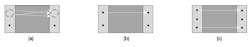
For that reason, it’s advisable to use single sharp-point probes for the current as well as for the sense contacts. This will set up a precisely defined current flow through the component, and repeatable ohmic value measurements (Fig. 1b). If the current requirements are simply too high to allow for the use of single sharp-point probes, then two probes may be employed for each current connection. This six-wire arrangement (Fig. 1c) has the additional benefit of setting up a symmetrical current flow pattern closer to that seen in operation on a PCB.
The standard contact X and Y spacings for the probe tips should be stated on the datasheet or otherwise advised by the manufacturer. The probe contact pattern should be centered in both directions on the component, because both lateral and longitudinal eccentricity will affect current-flow patterns and, hence, the ohmic value readings. Actual contact point positions may best be verified by measuring the locations of indentations in the terminations of a measured component.
The fixturing created to ensure accurate contact locations on the component will require maintenance to replace worn probe tips and that no misalignment arises. A repeatability and reproducibility study should be performed to ensure acceptable measurement variation with repeated use and alternative users.
In addition, the connection format should be specified. Usually, current contacts are on one side of the chip and voltage sense contacts on the other (Fig. 2a). A crossover format (Fig. 2b) also may be used and, for a given set of location point spacings, this will result in a lower ohmic-value reading.
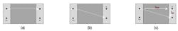
This becomes clear when we consider how the diagonal current-flow path may be resolved into a longitudinal and a lateral component (Fig. 2c). The longitudinal component is associated with most of the voltage drop, which is picked up by the sense terminals with the expected polarity. But the lateral component that gives rise to a smaller voltage drop is picked up by the sense terminals with inverted polarity, and therefore reduces the measured value.
Measurement System
The measurement system itself needs to be capable of measuring ohmic values in the 100-µΩ to 1-mΩ range with a level of uncertainty that’s small compared to the component tolerance. This may be achieved with a specialist micro-ohmmeter or with separate programmable current source and millivolt meter.
A typical current of 5 A in a 200-µΩ ±1% component under test will give rise to a sense voltage of 1 mV. The combined uncertainty of the current setting and the voltage measurement should be below 0.1%. The current-setting uncertainty can generally be kept very low, and if necessary, mitigated by independently measuring the actual current with a high-accuracy ammeter. This means that the voltage-measurement uncertainty would need to be 0.1% of 1 mV, which is 1 µV.
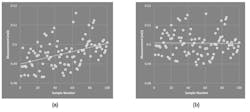
To mitigate thermal-drift errors, it’s advisable to leave the measurement system for at least an hour between switch on and use. Figure 3a shows measurement data obtained from a sample of resistors, which indicates an upward trend in mean ohmic value that could not be accounted for by any process changes in their manufacture. Figure 3b illustrates the repeat measurement results made after an appropriate stabilisation period.
Some thermal drift also may be seen within the individual measure cycle due to component heating. While the power dissipated in the element may be quite low, the point contacts can have relatively high resistance and thus generate heat that may affect the result. For this reason, the time interval between applying the current and measuring the voltage should be minimized and, if possible, standardized.
Two other methods are commonly employed to minimize the effect of error sources in such measurements. The first is the averaging of multiple readings taken over a defined time period, which is an integer number of power line cycles. This aims to achieve temporal cancellation of induced power line noise.
The second method is reversal of polarity during the measurement cycle, which aims to detect and correct for any imbalanced thermoelectric voltages. Dedicated micro-ohmmeters often have such functions built in, but a system made from separate source and measure equipment may require programming to achieve the same result.
Product-Specific Offsets
The ohmic value measured in the manner specified by the manufacturer, and taking into account all of the above-mentioned factors, may still differ from the value obtained when the part is mounted on the recommended pad layout. This occurs for two reasons.
First, the current flow through the resistor will not be the same when using one- or two-point contacts at each terminal as when using a solder joint. The latter—if voiding is low—connects to substantially the whole of the lower termination surface. Second, the voltage-sense separation normally needs to be somewhat greater than the minimum theoretically possible. This allows for tolerance in the location of probes relative to the resistor. In contrast, for a mounted part, the voltage-sense solder joints should always connect to the innermost points of the termination surfaces.
For these reasons, manufacturers typically have two standard methods for measuring ohmic values of sub-milliohm resistors. The first is to mount the part onto a defined Kelvin-connected test PCB, which is the definitive way to establish ohmic value. The second is to use probed connections, as described previously, and determine a standard mounting offset, normally negative, which is summed with the probe measured value to indicate the predicted mounted value:
Mounting offset = mounted value – probed value
This offset will vary depending on the termination dimensions, which in turn can be a function of the nominal ohmic value. Thus, it should be regarded as product-specific.
Critical Assembly Processes
Three assembly processes are vital to achieving low mounting-related errors in ohmic value: solder-paste printing, component placement, and reflow.
Solder Paste Printing
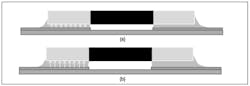
The thickness of solder in the finished solder joint has a direct bearing on the mounted ohmic value. This is because the vertically resolved component of current flow through the solder joint (Fig. 4a) is in a shared path with the voltage sense loop, which connects at the upper surface of the copper PCB pad. Consequently, increased solder thickness (Fig. 4b) will result in an increased mounted value.
The magnitude of this sensitivity may be estimated as follows, for a typical case:
ΔR/ΔL = 2 ρ/A
where ΔR is an incremental increase in mounting offset (mounted measured value – probe measured value) (Ω); ΔL is an incremental increase in solder thickness (m); ρ is the resistivity of the solder (Ωm); and A is the cross sectional area of the solder joint in the horizontal plane (m2).
For TT Electronics’ LRMAP2512-R0005FT4, 500 µΩ ±1% in a 2512 footprint, the value of A is approximately 8.32 mm2. And for SAC305 alloy solder, the value of ρ is 1.4 x 10⁻⁷ Ωm.
The factor of 2 reflects the fact that there are two terminations. This yields a sensitivity of:
ΔR/ΔL = 33.7 µΩ/mm
A typical stencil thickness is 130 µm. This thickness of solder would be predicted to result in a mounted value increase of 4.4 µΩ, which is about 0.9% of the nominal value. Variations in solder thickness of around ±20% around this value would then result in mounted value changes of nearly ±0.2%. That’s one reason why it’s not realistic to expect a ±1% tolerance on mounted values from a ±1% tolerance resistor.
Figure 5 shows the results of a study examining this sensitivity in the case of the example component referenced above. It yields a result of 28 µΩ/mm, which agrees broadly with the theoretical prediction. The fact that the empirical sensitivity is lower may be because conduction through the solder fillet has been ignored, and accounting for this would involve increasing the effective area A.
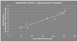
The same analysis may be applied to other components by substituting the underside termination areas (A) relating to them. It’s worth observing that large area and long-side terminations, which are often provided for reasons of thermal management to improve the thermal contact to PCB tracks, also have the benefit of lowering the sensitivity to variations in solder thickness.
Component Placement
The component-placement positional accuracy of current pick-and-place systems based on aluminium platforms is in the range 50 to 100 µm, reaching down to 20 µm for steel platforms.2 Once the tradeoff between accuracy and speed is applied, chip components are commonly placed with around 80-µm accuracy. This is perfectly adequate for normal resistors where mounting pad sizes are designed to accommodate this degree of variation.
However, when using sub-milliohm chip resistors, care should be taken to avoid an overhang of the termination on the interior edge of a mounting pad, beneath the component. This has the effect of bringing some current carrying termination inside the voltage-sense loop, thereby raising the mounted value (Fig. 6a). This would apply where the gap between the mounting pads exactly equals the gap between the terminations.
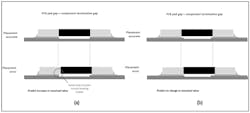
To overcome this potential problem, make the gap between mounting pads smaller than that between the terminations by an amount commensurate with the magnitude of the placement accuracy. Figure 6b shows how the same degree of longitudinal placement error has no effect on mounted value when this has been done.
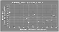
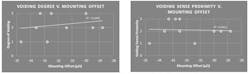
A practical study performed on TT Electronics’ LRMAP2512-R0005FT4 mounted on its recommended solder pads gave the results shown in Figure 7, indicating no correlation between mounting offset and longitudinal placement error up to about 100 µm. This indicated no correlation and therefore no indication of placement-error sensitivity.
A similar study on the effect of orientation angle errors also showed no sensitivity within the range ±2°. Transverse placement accuracy isn’t expected to cause issues provided the pad width is sufficient, and hence hasn’t been studied.
Reflow
Exposure to heat during the process of reflow can permanently affect the value of a resistor by altering the element material’s resistivity. This is typically established through initial testing by probed measurement and final testing by mounted measurement after reflow, to establish the value shift.
However, with sub-milliohm resistors that’s clearly problematic since a range of previously established factors can complicate the comparison in value between mounted and unmounted parts. The Resistance to Solder Heat test (e.g., 260°C ±5°C for 20s ±1s) for such resistors therefore tends to reflect the total value change. That’s due to a range of factors beyond the effect of heat exposure on the resistivity of the resistance element material.
If one wishes to study the effect of reflow on the element resistivity, a number of approaches apply. The first is to de-solder mounted parts and measure the final value in the same probe fixture used for the initial value measurements. Drawbacks of this approach are the presence of excess solder affecting the termination resistances and the fact that additional, uncalibrated heat exposure occurs during de-soldering.
An alternative is to probe on the upper surface of the resistor terminations both before and after reflow. This may not give the correct resistance value, depending on the degree of symmetry the resistor has about the horizontal plane, although this doesn’t matter for resistance change measurements. However, the presence of the PCB tracks can still affect the resistance of the terminations.
Possibly the best method is to perform a “dry” reflow, whereby the components are simply sent through a reflow process in a heat-proof container. Since the test conditions before and after are now identical, any resistance changes that are statistically significant (allowing for the repeatability of the probe measurement) may be ascribed to alloy resistivity shift.
A practical issue that can arise when reflowing components with larger termination areas is that of voiding within solder joints. If this is severe, it has the effect of reducing the cross-sectional area of the joint and thus increasing sensitivity to variations in solder thickness. Furthermore, there’s the possibility of voids having a greater effect on mounted value if they occur in the vicinity of the voltage-sense connection (Fig. 8a).
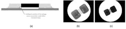
Figure 8b shows an X-ray of one of the mounted parts used in this study, which gave rise to concern that the mounted value might be affected. Other samples reflowed on a different line showed very low voiding levels (Fig. 8c).
The analysis of results from 10 parts is indicated in Figure 9, showing no correlation with degree of voiding or with proximity to the theoretically sensitive location. It may be concluded that voiding below 20% is not found to be problematic in practice.
Expected Ohmic Values During Life
Ohmic value, and how it may change of over the life of a sub-milliohm resistor, is one final consideration for designers. Reversible changes may occur because of the finite temperature coefficient of resistance (TCR), normally tested in a mounted state that includes the TCR for the solder between mounting pads and termination. Irreversible changes may occur due to changes in element resistance.
Performance data found in product datasheets enable designers to assess the maximum lifetime change in resistance value. Of most interest to designers is the maximum total error in resistance value at the end of product life, or before scheduled recalibration, if applicable. This is best illustrated by an example:
An LRMAP2512 resistor with 1% tolerance and TCR of 50 ppm/°C is to be soldered to a PCB for use in a laboratory-based power supply. The mean current through the resistor during operation will dissipate over 50% of the rated power. The operating temperature range inside the equipment is 20 to 50°C.
Short-Term Factors
- Tolerance: ±1%
- TCR: ±0.15% (±50 ppm/°C × 30°C)
- Soldering: ±0.3% typical
Long-Term Factor
- Load at Rated Power: ±0.3% typical, √ (12 + 0.152 + 0.32 + 0.32) = 1.2
Total Excursion Estimate: ±1.2% typical
Clearly if initial calibration can be used, this can eliminate tolerance- and soldering-process-induced errors, giving:
√ (0.152 + 0.32) = 0.11
Calibrated Total Excursion: ±0.11% typical
Summary and Conclusions
This article series demonstrates how the growing use of sub-milliohm chip resistors for current sensing creates a spectrum of challenges for the designer and the process engineer. The component format should first be selected to support the chosen thermal-management approach, with metal-element flat chip resistors having two terminals being the most cost-effective solution.
Next, it’s essential to design the PCB tracks and pads to meet the needs of Kelvin connection, heat dissipation, and avoidance of induced noise. If it’s necessary to make accurate measurements of unmounted components’ ohmic value, great care is needed to set up fixturing according to the manufacturer’s guidelines and to establish a capable test system. Lastly, the assembly processes of solder-paste application and pick-and-place require close control to ensure consistent solder thickness and component location.
With this insight, designers are well prepared for sub-milliohm design, tapping into simple and cost-effective design options that meet the demand for continually increasing power efficiency.
References
1. “Optimize High-Current Sensing Accuracy by Improving Pad Layout of Low-Value Shunt Resistors,” Marcus O’Sullivan; Analog Dialogue 46-06 Back Burner, June (2012); www.analog.com/analogdialogue.
2. “The Truth about Placement Accuracy,” Patrick Folmar; SST Semiconductor Digest; https://sst.semiconductor-digest.com/2000/04/the-truth-about-placement-accuracy/.
Read the rest of the Overcome the Challenges of Using Sub-Milliohm SMD Chip Resistors series.
About the Author
Stephen Oxley
Business Development Engineer, Fixed and Variable Resistors, Sensors and Specialist Components division, TT Electronics
Stephen Oxley is Business Development Engineer for the Fixed and Variable Resistors, Sensors and Specialist Components division at TT Electronics . He has a master’s degree in electrical and electronic engineering from Bath University, the U.K.
Comment About the Article
To join the conversation, and become an exclusive member of Electronic Design, create an account today!

Leaders relevant to this article: