When 1 + 1 = +3 (dB): Averaging ADC Channels to Improve NSD
This file type includes high resolution graphics and schematics when applicable.
Sampled data-acquisition systems using high-speed analog-to-digital converters (ADCs), such as those in communications infrastructure and electrical test-and-measurement applications, continue to have insatiable performance requirements for high signal-to-noise ratio (SNR) and low noise spectral density (NSD). While ADC design teams continue to turn out world-class converters, system engineers will continue to look for the last +3 dB of increased SNR and –3-dB reduction in NSD.
Averaging techniques can improve system performance through careful ADC configuration and back-end data processing. Although this can be achieved with discrete converter solutions, there are reasons why a more robust approach involves multichannel ADCs. In order to fully understand the approach, the benefits and associated tradeoffs must be weighed accordingly. These will be described along with the mathematical processing that makes it a reality.
Sampling at greater than twice the signal bandwidth, also known as oversampling, is a method that spreads noise power over a wider frequency band, effectively reducing noise density. However, if sampling at a higher rate is not an option, another approach uses multiple ADC channels or multiple ADCs that sample the same signal concurrently. The data from each converter can then be summed and averaged to extract a benefit similar to what’s provided by oversampling. Let’s look at some of the typical questions that pop up for this ADC configuration.
How does combining ADCs or ADC channels improve SNR and NSD?
By combining the signal outputs of two ADC channels and averaging them, the NSD is reduced similarly to that of a 2x oversampled condition. The electrical signal noise from two independent converters or channels is typically white and random. This means that, in general, the noise is predominantly uncorrelated from one channel to the other. The primary benefit of using a multichannel averaging approach is to average out this white random noise. Conversely, summing signals that are correlated in phase and frequency will additively combine their magnitudes.
When two uncorrelated signals (such as white noise) are summed together, they combine mathematically as a root-sum-square (RSS). This results in a magnitude increase by a factor of 1.414 for two equal amplitudes, instead of increasing by a factor of 2. Consequently, the result of combining two samples of the same signal is that the signal power will double (2x addition of the same signal) and the random noise will increase by only a factor of 1.414, or half the power of the signal. This yields an ideal increase in +3-dB signal power of the overall averaged SNR. Any mutually exclusive nonlinearities or noise within only one of the two ADCs, or one of the two input signal paths that’s not present in the other, will degrade some portion of the full +3-dB benefit.
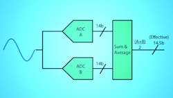
The output of two ADCs can be summed and averaged using back-end digital processing within an FPGA or digital signal processor. Alternatively, some multichannel ADCs can now provide the summation and averaging operation in real-time before the data is output from the converter. This reduces the need for further FPGA processing downstream.
This concept can be seen in Figure 1. Using two ADC channels within the same device provides the best path for success with this method, since the input full scale, gain, offset, and bandwidth are typically well-matched within a single piece of silicon. Using two separate discrete ADCs will make the exercise more challenging, because there’s greater potential for slight input and device mismatch, which will degrade the full +3-dB benefit.
Why is only an extra half-bit of resolution realized when averaging two ADCs and not a whole bit?
If we review the SNR math, we see that this combined input and average scheme gets an extra half of least significant bit (LSB) of resolution. Consider a simple case where two ADCs measure the same signal, including noise, and the outputs of each are averaged with each other.
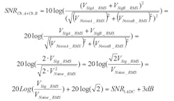
As shown above, when summed and averaged, ideally we get a 3-dB improvement in SNR.
The well-known relationship between SNR and ADC resolution (bits) based on quantization noise alone is as follows: SNR = 6.02 N + 1.76 dB (see ADI Mini Tutorial MT-229 for more information). As seen with this equation, every additional bit of resolution ideally increases SNR by about 6 dB. Therefore, the averaging technique of two ADCs improves SNR by about one-half of a LSB. Increasing SNR by 6 dB would require four averaged ADCs.
For applications in which noise is the main consideration, averaging provides an advantage by reducing NSD. The RSS summation of uncorrelated noise divided by the number of channels summed (which is effectively averaging) results in lower noise.
If Vnoise_1_RMS = Vnoise_2_RMS = Vnoise_RMS = noise on one ADC channel, then the average noise on two channels would be:
which is obviously a reduction. Using the reduced noise magnitude in the SNR calculation results in a 3-dB improvement. Another way to view the same phenomenon is shown by the following relation:
Negative SNR appears in the result as an independent parameter. As such, for a fixed, full-scale input amplitude, any increase in SNR corresponds to a dB-for-dB decrease in NSD with units of dBFS/Hz. The ideal result of combining and averaging: SNR increases by 3 dB, while NSD decreases by 3 dB.
Do spurs and harmonics from each ADC also sum together when two channels are combined?
If harmonics and/or spurs are part of the input signal shared by both ADCs, and the ADCs are completely identical (in an ideal case), the spurs would combine just like the signal. They would be 100% correlated and add directly to each other. Other frequency components not shared by both ADC inputs would not be 100% correlated.
Hypothetically, in the unlikely scenario where frequency components happen to be the same frequency and somehow 180 degrees out of phase with each other (inversely 100% correlated), they would destructively combine and cancel. In reality, complete signal cancellation like this is improbable. Practically, some portion of the frequency components from independent sources will be manifested at the ADC outputs.
In the case where harmonics are created independently by both individual ADCs, they are likely correlated with each other. That’s because a similar architecture mechanism is creating the harmonics in each of the identically designed ADCs.
What does an FFT look like using the channel averaged approach?
A fast Fourier transform (FFT) of two summed and averaged ADC channels will look appreciably similar to that of a single channel. The primary difference will be the performance benefit of increased SNR and lower NSD, when implemented correctly. For example, FFT plots of two independent single channels of a dual ADC each show about 69-dB SNRFS with an NSD of –153 dBFS/Hz (Fig. 2).
When the two channels are summed and averaged, the resulting performance is seen as 71.8-dB SNRFS and an NSD of –155.8 dBFS/Hz. In this case, the NSD and SNR benefit is only about 2.8 dB and not the entire 3 dB that’s available. The full performance isn’t realized in this case because small in-phase spurs and PCB imperfections between channels will not reduce with summing (as can be seen on the left side of Figure 3).The board design and layout was similar, but not completely matched, between Channel A and Channel B.Therefore, a portion of the channel-to-channel signal differences will still be present in the frequency domain as an averaged product.
Since the harmonic multiples of the fundamental signal are in phase and of similar amplitude between both channels, they will not correspondingly decrease in average power due to the processing. Consequently, an ADC’s spurious free dynamic range (SFDR), which is the dynamic range between the signal power and the next highest power harmonic, will not be improved using the averaging method.
What is the system penalty for using multiple ADCs or channels to improve SNR through averaging?
The signal source needed to drive two ADCs in parallel will require twice the power (twice the current), compared to the power needed to drive a single-channel ADC, in order to maintain a given voltage level seen at both of the ADC inputs. The phase, bandwidth, and amplitude of each will need to be matched to realize the full benefit of the +3-dB SNR boost.
When implementing an ADC configuration to achieve +3 dB in SNR, care must be taken to manage trace lengths to the ADC analog-input channels. Mismatches in trace length and bandwidth will cause degradation in performance (Fig. 4). If each channel signal is not exactly matched in phase and correlated, the full +3 dB of power increase will not be realized, as was seen in Figure 3. This degradation will manifest itself as spurs of non-signal energy.
Can ADC channel averaging be used within a narrowband digital downconversion (DDC) operation?
We discussed the noise spectral density for a Nyquist-rate ADC as: NSD(dBFS/Hz) ≡ –SNR –10Log(Fs/2). However, there are several applications where the primary signal of interest is located only within a small bandwidth (BW). This narrow bandwidth can be much smaller than the full ADC Nyquist sampling bandwidth. Here, digital filtering can be used to filter the noise outside of this bandwidth. Processing can be done using a DDC stage to decimate, tune, and filter the data before it is output from a Nyquist-rate ADC (Fig. 5). Our SNR calculation must then include a correction factor for the filtering that accounts for the processing gain achieved from the removal of the filtered noise.
Ideal SNR (with processing gain) = 6.02*N + 1.76 dB + 10log10(Fs/(2*BW)), where N is the ADC resolution in number of bits, Fs is the ADC sampling frequency, and BW is the narrow decimated sample bandwidth of interest. The two-channel averaging mode can also be used when implementing a DDC function, provided that each of the ADC channel’s digital-processing stages have the same latency, filter bandwidth, and pass-band flatness:
SNRCh.A+Ch.B = 6.02*N + 1.76 dB + 10log10(Fs/(2*BW)) + 3 dB
NSDCh.A+Ch.B = –SNRCh.A+Ch.B – 10log10(Fs/(2*BW))
Depicted are FFT plots of two independent single channel ADCs that use a decimation factor of 16 with a digital filter and a numerically controlled oscillator (NCO) as a mixer (Fig. 6). Independently, each channel shows 81-dB SNRFS with an NSD of –164 dBFS/Hz within the bandwidth of interest. For every power-of-2 reduction in BW, there’s a corresponding 3-dB increase in SNR, due to the digital filtering of the out-of-band noise.In this case, the decimated BW of interest is 1/16th of the sample rate, which achieves an ideal processing gain of 12 dB.
When the two channels are summed and averaged, the resulting performance within the band is seen as 83.8-dB SNRFS and an NSD of –166.8 dBFS/Hz. In this case, the NSD and SNR benefit is only about 2.8 dB and not the entire 3 dB available. Again, as in the Nyquist-rate summation scenario, the reason that the full performance isn’t realized is due to small in-phase spurs and crosstalk from non-ideal board matching that will not cancel with summing and averaging.
The summing and averaging of two channels within an ADC can provide an ideal +3-dB boost in SNR. Un-correlated white noise is averaged out between the two channels and correspondingly reduces the ideal NSD by 3 dB. Careful consideration for the system board layout is needed to maintain matched phase, amplitude, and bandwidth to both ADC channels to achieve the maximum signal power increase. This technique can also be used in conjunction with matched digital downconversion stages in the cases that don’t require the full Nyquist bandwidth. The AD9684, a dual, 14-b, 500-Msample/s ADC from Analog Devices, offers this feature internally, so digital post-processing for the signal gain is not needed.
References:
Kester, W., Taking the Mystery out of the Infamous Formula, "SNR = 6.02N + 1.76dB," and Why You Should Care, MT-001, retrieved from Analog Devices Training Seminars: http://www.analog.com/media/en/training-seminars/tutorials/MT-001.pdf
Man, C., Quantization Noise: An Expanded Derivation of the Equation, SNR = 6.02 N + 1.76 dB, MT-229, retrieved from Analog Devices Training Seminars: http://www.analog.com/media/en/training-seminars/tutorials/MT-229.pdf
Reeder, R., Looney, M., and Hand, J., Pushing the State of the Art with MultiChannel A/D Converters, retrieved from Analog Devices Training Seminars: http://www.analog.com/library/analogDialogue/archives/39-05/multichannel.html
CN-0249 14-Bit, 125 MSPS Quad ADC with SNR Enhanced by Post Digital Summation, retrieved from Analog Devices Circuit Notes: http://www.analog.com/media/en/reference-design-documentation/reference-designs/CN0249.pdf
About the Author
Doug Ito
Applications Engineer, High Speed A/D Converters
Doug Ito is an Applications Engineer for the High Speed A/D Converters team at Analog Devices Inc. (San Diego, Calif.). He earned a Bachelor’s in electrical engineering from San Diego State University. Doug is a member of EngineerZone’s High-Speed ADC Support Community. Feel free to send your questions to DougI on Analog Devices EngineerZone Online Technical Support Community.
Ian Beavers
Product Engineering Manager, Automation Energy and Sensors, Analog Devices
Ian Beavers is a product engineering manager for the Automation Energy and Sensors Team located at Analog Devices, Greensboro, N.C. He has worked for the company since 1999. Ian has over 20 years of experience in the semiconductor industry. He earned a bachelor’s degree in electrical engineering from North Carolina State University and an M.B.A. from the University of North Carolina at Greensboro.
Voice Your Opinion!
To join the conversation, and become an exclusive member of Electronic Design, create an account today!

Leaders relevant to this article:


