Download this article as a .PDF
Silicon’s 20th Century dominance in power electronics applications has been eroding for some time now. As engineers extract dwindling amounts of additional performance from silicon ICs, they are looking to wide-bandgap (WBG) materials to develop next-generation power electronics. Examples include silicon carbide (SiC) and gallium nitride (GaN). Materials that have a wide bandgap are inherently applicable in high-power electronics, as they have a higher breakdown voltage and are able to run at higher temperatures when compared to materials with narrow bandgaps, such as silicon.
SiC and GaN also offer the potential for smaller, more robust power devices, which switch faster and are more energy-efficient than Si-based devices. SiC and GaN products, in demand for electric-car and mobile-device applications, perform much better than Si in reducing on-state resistance and shrinking package size. This results in faster charging, lower power consumption, and more efficient energy conversion. Generally speaking, SiC power semiconductor devices are being specified for applications with high power capacity (in excess of 600 V) and GaN for applications involving medium to low-power capacities.
Silicon carbide has become an attractive alternative to Si in applications requiring efficient high-voltage, high-frequency power conversions. SiC power devices operate at higher switching speeds and higher temperatures with lower losses than conventional silicon. In addition, SiC allows inverters and other energy-conversion systems to be built with improved power density and energy efficiency at lower cost. Almost all the OEMs and Tier-1s are using or testing SiC devices in electric and hybrid electric vehicles (EVs and HEVs).
Similarly, GaN possesses high breakdown voltage and low conduction resistance characteristics, thereby enabling high-speed switching and miniaturization. Unlike conventional Si transistors, which require bigger chip areas to reduce on-resistance, GaN devices have smaller sizes (and lower parasitic capacitance) for high-speed switching. Miniaturization is possible in part because of the smaller passive components needed.
As evidence of the growing maturity of WBG materials, JEDEC—a global leader in developing open standards for the microelectronics industry—just formed a new committee: JC-70 “Wide Bandgap Power Electronic Conversion Semiconductors.” This team is helping to create the mature industry infrastructure that customers need to design power supplies. Led by interim chairs from Infineon, Texas Instruments, and Wolfspeed, the new JC-70 committee will initially have two subcommittees (yes, you guessed it): Gallium Nitride and Silicon Carbide. Both will focus on Reliability and Qualification Procedures, Datasheet Elements and Parameters, and Test and Characterization Methods. Let’s now look at recent developments in SiC and GaN one at a time.
GaN: Servo Motors, Laptop Adapters, Radar, PAs, and High-Speed Wireless
According to a new report from MarketsandMarkets, “Gallium Nitride Semiconductor Device Market—Global Forecast to 2023,” the GaN semiconductor device market is expected to reach $22.47 billion by 2023. It will chalk up a CAGR of 4.6% between 2017 and 2023. In 2016, optoelectronic devices held the largest market share. (GaN LEDs are widely used in laptops and notebooks, televisions, and signs). Yet the market for GaN-based inverters for motor drives is expected to grow significantly during the forecast period. Indeed, another market research firm, Yole Développement, is even more optimistic. While the power-supply segment will remain the biggest application for GaN, it suggests that the data-center market is adopting GaN solutions as well—driving a 114% CAGR for power supplies through to 2022.
The advantages of high-voltage GaN field-effect transistors (FETs) are best seen when used in power electronics systems including power supplies, servo motors, and photovoltaic inverters. Yaskawa Electric Corp.’s Σ-7 F is the first servo motor to use high-voltage (HV) GaN, in this case provided by Transphorm (and precipitated by a $15 million investment in Transphorm from Yaskawa Electric). The AEC-Q101-qualified, 650-V GaN semiconductors enabled Yaskawa to develop an integrated servo motor half the size of a similar design using Si technology. The key achievement here is that the Σ-7 F integrates the servo amplifier with the servo motor itself. According to Yaskawa, the topology will be deployed across its full Σ-7 F product line, which currently includes three servo motors ranging from 100 to 400 W.
By integrating the driver in the same package, as Texas Instruments has done with its TIDA-00915 reference design, it’s possible to reduce parasitic inductances and optimize switching performance. This approach reduces power loss, allowing the designer to downsize the heat sink. Such space savings are beneficial for compact servo drives and motor-integrated drives. Operating the inverter at a high switching frequency of 100 kHz reduces the current ripple, which improves torque ripple when used with low-inductance motors. The three-phase inverter design for driving 200-V AC servo motors (with 2 kWPEAK) is built around six of TI's LMG3410 600-V, 12-A GaN power modules. They allow switching up to five times faster than silicon FETs, while achieving efficiency levels said to be greater than 98% at 100 kHz and 99% at 24 kHz pulse width modulation (PWM).
Designed to help engineers evaluate USB power-delivery (PD) adapters and dongle solutions featuring power and data, Navitas Semiconductor has developed what is reportedly the smallest 65-W USB-PD laptop adapter. It minimized the size, weight, and cost of transformers, filters, and heatsinks through the use of AllGaN Power ICs. The part delivers 65 W in only 2.7 in.3 and weighs only 60 g. By contrast, existing silicon-based designs can require 6 to 7 in.3 and weigh over 300 g. The new reference design uses its GaN power ICs in an active-clamp-flyback (ACF) topology running 3x to 4x faster and with 40% lower loss than typical adapter designs. The firm says that its AllGaN 650-V platform process design kit (PDK) monolithically integrates GaN power FETs with logic and analog circuits, enabling smaller, high-energy-efficiency and lower-cost power for mobile, consumer, enterprise, and new energy markets.
A promising approach to long-distance, high-capacity wireless communications is to utilize the 75 to 110 GHz W-band and increase output with a transmission power amplifier. Fujitsu has succeeded in developing a power amplifier for use in W-band transmissions that offers both high output power and high efficiency, improving transistor performance through the reduction of electrical current leakage and internal GaN high-electron-mobility-transistor (HEMT) resistance. The company has achieved 4.5 W per millimeter of gate width, which is said to be the world's highest output density in the W-band. In addition, it has confirmed a 26% reduction in energy consumption compared to conventional technology.
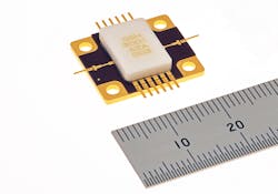
The latest GaN-on-SiC HEMTs from Cree’s Wolfspeed (Fig. 1) comprise a series of 28-V RF power devices that can operate to 8 GHz. The new devices were developed using Wolfspeed’s 0.25-µm GaN-on-SiC process. They are designed with the same package footprint as the previous-generation 0.4-µm devices, making it easy for RF design engineers to use them as drop-in replacements. The new GaN HEMTs are said to deliver 33% higher frequency operation to 8 GHz (from 6 GHz) as well as a 5% to 10% boost in operating efficiency compared to Wolfspeed’s earlier-generation devices. The higher efficiency and bandwidth capability make these devices well-suited for a range of RF power amplifier applications including military communications systems, radar equipment, electronic warfare (EW), and electronic countermeasures (ECMs).
1. Shown are the GaN HEMT MMIC semiconductor process components from Wolfspeed. On the subject of frequency bands per amplifier, the company’s literature says, and we kid you not, that it has “more bands than Woodstock.”
With the continuing development of GaN HEMTs, new topologies and control methods are challenging classic power-supply architectures. In soft switching applications, for instance, GaN HEMTs have the potential for very high switching frequencies. In contrast, silicon-based counterparts are limited to low and moderate switching frequencies. An example is satellite networks, which are used for high-speed communication during natural disasters and in areas where ground networks are difficult to construct. Currently, they are implemented mainly in the C-band (4 to 8 GHz) and Ku-band (12 to 18 GHz).
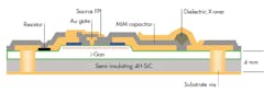
Higher frequencies are increasingly being explored, however. In response, Mitsubishi Electric has launched a Ka-band (26 to 40 GHz), 8-W GaN HEMT monolithic microwave integrated circuit (MMIC) amplifier for satellite earth stations (Fig. 2). Its new GaN-HEMT MMIC, which offers low distortion and an output power rating of 8 W, boasts a small footprint that will help to downsize power transmitters. Features include one-chip integration of amplifier transistor circuits, matching circuits, and a built-in distortion-reducing linearizer.
2. Solutions like the MGFG5H3001 Ka-band GaN-HEMT MMIC from Mitsubishi will help meet the growing demand for higher-frequency satellite deployments. The company began shipping samples in November.
SiC: Inverters, Server Power, and Photovoltaics
Today, SiC technology’s added value is widely understood and accepted by the power electronics community. Yole’s analysts peg CAGR at 28% through 2022 (Fig. 3). Part of the appeal of SiC comes from its physical properties. For example, where silicon has a breakdown electric field of 0.3 MV/cm, SiC can withstand up to 2.8 MV/cm. Its internal resistance is 100 times smaller than that of silicon. As a result, applications can handle the same level of current using a smaller chip and, in turn, smaller systems.
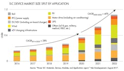
3. Yole Developpement analysts pull no punches. In 2016, they said the SiC power business was “concrete and real, with a promising outlook.” This year, they added,“The trend has not changed in 2017 and even more, the SiC industry is going further.”
Recently, Rohm developed an all-SiC, 1200-V, 600-A power module integrating SiC Schottky barrier diodes (SBDs) and MOSFETs. The module achieves a rated current of 600 A by utilizing a new package featuring a revised internal structure and optimized heat radiation design. In doing so, it enables support for higher-power applications. This half-bridge module is suitable for the following applications: motor drive, inverter, converter, photovoltaics, wind-power generation, and induction heating equipment. Compared to IGBTs, the SiC MOSFET offers much faster switching. At a chip temperature of 150°C, Rohm claims that the part offers a 64% reduction in switching losses (Fig. 4). A new package has a flatter baseplate that decreases contact resistance by 57% and inductance by 23% (compared to earlier products) by optimizing the placement of the SiC device inside the package. According to the company, the “G Type” package decreases switching loss by 24% under the same surge-voltage drive conditions.
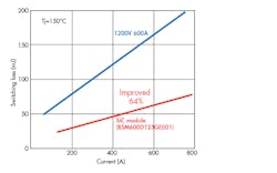
4. According to Rohm, SiC power modules equipped with its SiC SBDs and MOSFETs make it possible to reduce switching loss by 64% (at a chip temperature of 150°C) vs. IGBTs at the same current rating. (Source: Rohm)
The Infineon 650-V G6, as the name implies, represents the sixth generation of the company’s CoolSiC Schottky diodes. These devices are built upon the characteristics of its G5 series, but feature a new layout, cell structure, and proprietary Schottky metal system. The G6 diodes are designed to complement Infineon’s 600-V and 650-V CoolMOS 7 families. Aimed at current and future applications in server and PC power, telecom power, and photovoltaic inverters, the CoolSiC 650-V G6 boasts an industry benchmark V F (1.25 V), and a Q c x V F figure of merit (FOM), which is 17% lower than the previous generation, according to Infineon. In addition, the new G6 diode leverages two of silicon carbide’s strong characteristics: temperature-independent switching behavior and no reverse recovery charge.
SiC Schottky diodes have approximately 40 times lower reverse leakage current than PN silicon Schottky diodes. Littelfuse, which got into the SiC game through its acquisition of Monolith Semiconductor, has come out with a new generation of 1200-V SiC Schottky diodes with current ratings from 5 to 40 A. With negligible reverse recovery, the LSIC2SD120 Series—the Monolith/Littelfuse partnership's first product introduction--reduces switching losses (compared to Si bipolar diodes) to boost system efficiency. The switching behavior of the diodes is temperature-independent and the operating junction temperature is 175°C. These aspects enable a larger design margin and reduced thermal management requirements. Target applications are EV charging stations, solar inverters, and switch-mode power supplies.
Using its second-generation SiC MOSFET technology, STMicroelectronics has introduced a 650-V, 22-mΩ (typically at 150 °C) SiC power device. The main features of this product include low on-resistance per unit area and better switching performance. The variation of both RDS(on) and switching losses are said by ST to be almost independent from junction temperature. When employed in the EV/HEV main inverter, the company reports that the part increases efficiency by up to 3% compared with an equivalent IGBT solution. This translates into longer battery life and a lighter power unit. ST’s SiC MOSFETs also feature what the company claims is the industry’s highest junction-temperature rating of 200°C. This leads to higher system efficiency, which reduces cooling requirements and PCB form factors, simplifying thermal management.
Gaining Momentum
Efficiency, power density, and the reduction of system cost are key drivers behind the use of the WBG materials SiC and GaN. While some application areas tend to be early adopters for new technology (if benefits outweigh risks), many others are now following as these materials move into more mainstream applications. As additional suppliers enter the market, increased production will drive down costs. Those cost benefits—taken together with quality and reliability gains—will push the rapidly maturing SiC- and GaN-based topologies to the tipping point, even in cost-sensitive applications.

About the Author
Murray Slovick
Contributing Editor
Comment About the Article
To join the conversation, and become an exclusive member of Electronic Design, create an account today!

Leaders relevant to this article: