Noise Considerations in ADC Signal Chains

What you'll learn:
- Defining noise bandwidth.
- Resistor noise and amplifier noise contributions.
- Clocking noise contributions.
- Power-supply noise contributions.
- Putting all of the noise contributions together.
Many noise sources can plague high-speed radio-frequency (RF) analog signal chains, making design considerations that much more challenging. Both megahertz and sub-terahertz sampling-rate converters have analog, clock, and power inputs, which realize the converter as a multi-input “mixer” with a digital back end.
With continuously constrained converter headroom, maintaining a noise spectral density of 150 dBFS/Hz is challenging with each new design. That’s why it’s paramount to recognize the importance of the surrounding noise contributions that may erode performance within the entire signal chain.
Indeed, there’s an extensive range of noise principles—too many to even list. This article addresses some basic noise principles and how to apply them to each analog-to-digital converter (ADC) input node to minimize any noise convolving onto the output spectrum.
Defining Noise Bandwidth
Noise bandwidth isn’t the same as the typical –3-dB bandwidth you may be accustomed to, such as an amplifier’s bandwidth or filter cutoff point. Noise takes on a rectangular shape to specify the integration of the bandwidth. (Without going into a lengthy derivation in noise bandwidth, see Reference 1.) When integrating the noise in rectangular form, for a standard first-order system, the noise bandwidth will be 57% larger than the –3-dB cutoff. For example, 150 MHz of bandwidth determined by a second-order anti-aliasing filter (AAF) located between an amplifier and an ADC will result in a noise bandwidth of 183 MHz, or 1.22*150 MHz.
The table lists the integration noise bandwidth for multiple order systems, which a designer can use to help set final calculations in the signal chain.
Resistor Noise and Amplifier Noise Contributions
The second noise fundamental to consider is resistor noise. Think of resistors as very small heating elements that generate thermal noise. Even though their contributions to noise are small, they can add up quickly if high-value resistors are used. Resistive noise contributions add up even more quickly if high-value resistors are wrapped around an amplifier in a gain configuration.
Equation 1 defines resistive noise or error as:
Er = √(4kTRΔf) (1)
where:
- k is 1.38 ´ 10-23W/s/K (Boltzmann’s constant)
- T is 290 Kelvin
- R is the resistance in ohms
- Δf is the noise bandwidth of the system in hertz
Therefore, 1 kΩ = 4 nVRMS/Hz for 1-Hz bandwidth; resistor noise is equal to 4 nV/√(Hz) per 1 kΩ. The designer can use this reference ratio when calculating noise contributions with resistors that are wrapped around an amplifier to enable gain.
Amplifiers are active devices, which means that they need a power supply to function properly. In most signal-chain noise analyses, the goal is to find or calculate the amplifier’s referred-to-output (RTO) noise, which is the noise value required to complete the signal-chain noise analysis and how RTO noise affects the ADC’s overall performance.
>>Download the PDF of this article

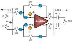
For example, using Figure 1 as a generic amplifier model, if the amplifier’s datasheet specifies a bandwidth of 320 MHz, that equates to a noise bandwidth of 1.57*(3-dB bandwidth), or 502.4 MHz per the previous section.
Then find the amplifier’s voltage- and current-noise contributions, which are located in most amplifier datasheets. In this case:
Voltage noise or En = 5 nV/√(Hz)
Current noise or In = 2 pA/√(Hz)
The next step is to calculate the error ratios for the input (Ei) and feedback (Ef) resistive elements:
Ei = (550/1,000) ´ 4 nV = 2.2 nV/√(Hz)
Ef = (557/1,000) ´ 4 nV = 2.23 nV/√(Hz)
To round out the amplifier noise analysis, compute the input resistive voltage-noise, the amplifier’s voltage-noise, and current-noise contributions based on the resistors used in Figure 1’s noise model:
RINPUT voltage noise = Ei × (1 + 557/605) = 4.23 nV/√(Hz)
Amplifier voltage noise = En × (1 + 557/605) = 9.6 nV/√(Hz)
Amplifier current noise = (In × 557 || 605**) × (1 + 557/605) = 1.11 nV/√(Hz)
**“557 || 605” denotes the total resistance of 557- and 605-Ω resistors in parallel.
Now, root sum square (RSS) these terms to compute the final RTO noise value:
Front-end noise = √((RINPUT voltage noise)2 + (Amp voltage noise)2 + (Amp current noise)2 + (Ef)2) = √((4.23 nV2 + 9.6 nV2 + 1.11 nV2 + 2.23 nV2)) = 10.8 nV/√(Hz)
Total noise = √(Noise bandwidth) × front-end noise = √(502.4 MHz) × 10.8 nV = 241.7 μVRMS
Note that amplifiers are different from operational amplifiers, simply because they typically include resistive elements internal to their package. Thus, the noise contribution is the overall noise given in the respective amplifier’s datasheet. An amplifier with included resistors usually specifies the noise as referred-to-input (RTI) noise. Using the gain in the amplifier circuit enables conversion of the RTI number to RTO noise.
For example, if a specific amplifier in the RF signal chain has 1.3 nV/√(Hz) of RTI noise, and the designer wants to use a gain of 16 dB to translate the input signal more closely to the full scale of the ADC, see Equation 2:
RTI = 1.3 nV/√(Hz),
gain = 16 dB
thus
RTO = 1.3n x 10 (16/20) =8.2 nV/√(Hz) (2)
The designer will need to know the RTO noise of the amplifier to fully calculate the RF signal-chain noise of the entire system. This number will become significant later when summarizing all of the signal-chain noises together.
References 1 and 2 offer more information about noise bandwidth, resistor noise, and amplifier calculations and considerations.
Clocking Noise Contributions
Another important noise contribution to overall signal-chain performance is clock noise or jitter. This contribution affects the performance of an ADC at its core and can quickly degrade its rated dynamic range capability if the right clocking signal chain, clock oscillator, voltage-controlled oscillator—or all three—aren’t well-defined.
With just a basic understanding of how to factor in clock noise and an initial assumption that clock noise and jitter are broadband, it’s possible to get a good sense of the influence that this metric may have on the total system’s signal-chain performance.
To calculate jitter, set the lower integration bandwidth limit to a value close to DC to consider the entire phase-noise profile of the clock. It’s recommended to use at least the ADC sampling frequency (Fs), and for even better analysis, 2 × Fs for the integration bandwidth. Many times, 2 × Fs is more appropriate to understand the broadband noise contribution and reach the sampling clock’s noise floor (Fig. 2).
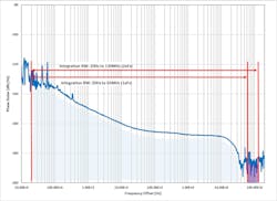
For example, if the ADC is sampling at 65 MSPS, the integration bandwidth ranges from 20 Hz to at least 65 MHz (or up to 130 MHz for a more detailed noise consideration). Simply use the defined integration broadband jitter noise in seconds (preferably femtoseconds or below) and the analog input frequency or intermediate frequency (IF) of interest. The maximum error occurs when the clock amplitude is at its highest, assuming a sine-wave input.
Equation 3 calculates the root mean square (RMS) voltage error—that is, the sampling clock’s additive noise to the RF signal chain. For example, a 30-MHz analog input IF and a clock jitter of 100 fs yields a broadband voltage noise or error of:
18.8 µV or Vn = (2π) × (30 MHz) × (100 fs) (3)
References 3 and 4 offer more information about clocking considerations, and how these relate to ADC and RF signal chain performance.
Power-Supply Noise Contributions
Let’s explore how power-supply noise can influence RF signal-chain performance. Typically, in an analog supply domain (AVDD), the analog power domains are the most sensitive to power-supply noise, so this supply type will be used as an example.
Similar to all active devices that require a power supply connected to them, all regulator types (low-dropout regulators and switchers) have some sort of noise. This noise, depending on how dominant it is, can also affect the ADC’s performance, just like an amplifier’s noise or anything else in the RF signal chain. Here’s how.
As with clock noise, regulator noise can couple through the power-supply pins of the ADC or any active device that requires a power-supply connection. In the clock example, the internal circuitry of the clocking nodes is tied into the sample-and-hold structures internal to the analog inputs of the ADC. This makes it the perfect place for any noise or coupling through the clock pins to find its way into the internal signal path of the ADC.
The coupling path has almost zero attenuation in this case. In the power supply’s case, however, notice that the internal circuitry from the power-supply pin of the ADC includes an attenuation symbol (Fig. 3).
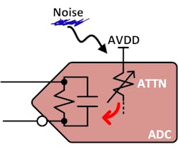
This symbol represents the ADC’s rejection of any noise or signal coupling through the power pins, which is measured as the power-supply rejection ratio (PSRR). Ultimately, this attenuation defines the amount of coupled rejection, or PSRR, from the internal circuit design inside the ADC. Some circuit design topologies allow for less noise attenuation than others; therefore, more noise can leak into the ADC’s digitization path, degrading the ADC’s performance.
To quantify the regulator’s noise and its effect on the ADC, the designer can use the regulator’s measured noise band, which is usually found in the regulator’s datasheet. For example, a regulator can have 225 μV of noise over a 100-kHz bandwidth. Assuming that the noise is flat or Gaussian, the designer can use this specification to estimate how it might contribute to the overall performance of the ADC signal chain.
However, the ADC’s power-supply rejection (PSR) number also needs to be known. Sometimes this number is in the datasheet or is measurable on the lab bench.
In most cases, the PSR is around −40 to −60 dB over the first Nyquist in the AVDD, which is typically the most sensitive converter supply. In this case, let’s assume −40 dB for simplicity. The effective noise contribution is then 7.12 nV or 225 μV/√(100 kHz) × 10(−40/20).
Keep in mind that this is only for one supply domain. The designer will need to evaluate all supply domains in the same manner, and each domain may have different PSR values within the ADC, amplifier, and so on.
References 5 and 6 offer more information and insight on power-supply noise and PSR and its effects on ADCs (see References 6 and 7).
Putting All of the Noise Contributions Together
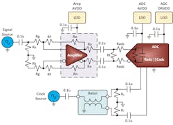
Figure 4 shows a simplified RF signal-chain block diagram noise model that builds on the preceding discussion.
The last step is to find the ADC’s noise contribution in the signal chain. For example, an ADC may have an analog input full scale of 1.75 V p-p differential, while the datasheet lists the signal-to-noise ratio (SNR) as 71.7 dBFS. By back-calculating noise out of the SNR equation, Equation 4 reveals the thermal noise:
SNR = 20 × log(full scale (VRMS)/thermal noise (VRMS)) (4)
or
71.7 dB = 20 × log(((1.75/2)/√(2))/ thermal noise (VRMS))) = ADC thermal noise = 161 µVRMS
Next, determine the noise contributions as previously described for the rest of the power supplies.
The AVDD contribution for the ADC analog supply is 7.12 nVRMS.
Do the same for the digital supply domain (DRVDD) of the converter and the AVDD of the amplifier. In these calculations, the PSRR of the DRVDD of the converter is −80 dB and the PSRR of the amplifier’s AVDD is −60 dB:
Amplifier AVDD = 450 μV/√(100k) × 10(−60/20) = 1.42 nV
ADC AVDD = 225 μV/√(100k) × 10(−40/20) = 7.12 nV
ADC DRVDD = 225 μV/√(100k) × 10(−80/20) = 71.2 pV
To find the total noise contribution of all of the power supplies, simply RSS these three noise sources, which gives a total of 7.2 6 nVRMS or √(7.12 nV2 + 71.2 pV2 + 1.42 nV2).
From the previous amplifier example, the RTO noise is 8.2 nV/√(Hz) with a gain of 16 dB.
Typically, the designer will use an AAF between the output of the amplifier and the input of the converter. Otherwise, all broadband noise from the amplifier folds back in-band. Therefore, by limiting this noise with an AAF, the assumption becomes that the bandwidth of the filter is 105 MHz (−3-dB cutoff), because the ADC is sampling at 250 MSPS and has a Nyquist band of Fs/2 or 125 MHz.
Generally, to capture the entire Nyquist band of interest without folding noise back in, a general estimate of 85% of the Nyquist band can be assumed. Therefore, the AAF can be designed to be somewhat smaller.
In this example, a two-pole inductor-capacitor filter (second-order system) for the AAF implementation was used, yielding a noise bandwidth of 105 MHz × 1.22 = 128.1 MHz. The noise contribution of the amplifier is thus 92.8 μVRMS or 8.2 nV × √(128.1 MHz).
Finally, collect all of the noise sources derived in the example signal chain using the following standard SNR equation (Equation 5) and RSS them all together:
SNR = 20 × log((FSRMS)/(√(ADC µVRMS2 + Amp µVRMS2 + LDO nVRMS2 + Clock µVRMS2))) (5)
or
SNR = 20 × log((1.75/2)/√(2))/(√(161 µVRMS2 + 92.8 µVRMS2 + 7.26 nVRMS2 + 18.8 nVRMS2 ))) = 70.4 dB
This example identifies the total signal dynamic range in terms of the converter’s SNR. By reviewing these contributions in more detail, the designer can easily see what part of the signal chain is “donating” the highest noise contribution aside from the ADC’s own internal thermal noise. In this case, the amplifier’s noise is the largest contributor. It helps the designer understand each individual noise source impact and offers insight into the tradeoffs one needs to make to improve overall system performance.
References 7, 8, and 9 offer more information about summarizing ADC errors and understanding these tradeoffs at the AAF and system level.
Conclusion
Understanding signal-chain noise tradeoffs and root causes of noise can lead to easier design tradeoffs upfront when designing high-speed signal chains. Knowledge of how both active and passive devices interact within a signal chain in terms of noise illuminates how to predict the total dynamic range performance outcome, in terms of SNR, of the entire signal chain. Keep these principles in mind when calculating signal-chain dynamic range tradeoffs. Otherwise, the next design may go noisy.
A noise calculation spreadsheet is attached, here, for Electronic Design readers’ convenience, courtesy of Texas Instruments.
References
1. Low Noise Electronic System Design, C.D. Motchenbacher, June 1993.
2. SLVA417: “DC Output Errors in a Fully-Differential Amplifier,” John Miller, TI.com.
3. SBAA653: “Practical Clocking Considerations That Give Your Next High-Speed Converter Design an Edge,” Rob Reeder and Andrea Vallenilla.
4. AN-501: Brad Brannon, Analog Devices Inc.
5. SLYT811: “Clutter-free power supplies for RF converters in radar applications (Part 1),” Rob Reeder and Neeraj Gill.
6. SLYT815: “Clutter-free power supplies for RF converters in radar applications (Part 2),” Rob Reeder and Neeraj Gill.
7. “Unraveling the full-scale mysteries of your RF converter’s analog inputs,” Rob Reeder, Electronic Products, Nov. 2019.
8. “Breaking down accuracy errors in a precision high-speed ADC signal chain,” Rob Reeder, Analog Design Journal, Sept. 2020.
9. “How anti-aliasing filter design techniques improve active RF converter front ends,” Rob Reeder, Analog Design Journal, April 2024.
>>Download the PDF of this article
About the Author

Rob Reeder
Application Engineer, High-Speed Converters, Texas Instruments
Rob Reeder is currently the application engineer for High-Speed Converters at Texas Instruments (TI) in Dallas. Rob’s prior experience includes RF design at Raytheon Missile Systems in Tucson, Ariz., including analog receivers and signal-processing applications. He was also a system application engineer with Analog Devices in the High-Speed Converter and RF Applications Group in Greensboro, N.C., for over 20 years.
He has published over 130 articles and papers on converter interfaces, converter testing, and analog signal chain design for a variety of applications. Rob received his MSEE and BSEE from Northern Illinois University in DeKalb, Illinois, in 1998 and 1996, respectively. When Rob isn’t writing papers late at night or in the lab hacking up circuits in the lab, he enjoys hanging around at the gym, listening to EDM, building rustic furniture out of old pallets, and, most importantly, chilling out with his family.
Comment About the Article
To join the conversation, and become an exclusive member of Electronic Design, create an account today!

Leaders relevant to this article: