Flying probes take on the challenge of loss of test access
Today’s electronic circuit-board technology is posing a big challenge to in-circuit test techniques because of the disappearance of access. As a result, a shift from bed-of-nail to flying-probe equipment is ongoing. While the main drives for this shift are consumer products for the exploding Internet of Things market, manufacturers of high-performance professional products are also following this trend. Extreme examples are costly, high-quality, and high-reliability products such as boards hosted on satellites. Here the flying probe is challenged to overcome physical access limitations, enhance the accuracy and repeatability of probing, prevent any mechanical or electrical degradation, and ensure thoroughness of test. This article addresses the solutions to these requirements based on a successful customer’s experiences.
If one wishes to describe what electronic technology is doing today, this can be summarized in one sentence: products do more, they do it faster, they weigh less, and they are physically smaller. How has technology achieved these results? Through drastic evolution on PCB manufacturing, with new packaging (BGA, COB, CSP, etc.) and high-density interconnect to allow electronics to shrink in size while expanding technology, versatility, quality, and speed.
All that has a price to be paid: test access for conventional bed-of-nails equipment is reduced or disappearing. As a consequence, in the last ten years we have seen a substantial shift of test-equipment investments from conventional bed-of-nails to flying-probe in-circuit test systems. The main reason for this shift is, as said, test access, and consequently cost/feasibility of fixtures and fault coverage. While test-fixture technology finds its limits hitting test pads no smaller than 25 to 30 mils, flying probes can easily and reliably bring this number down of an order of magnitude and even allow safe access on components’ pads when test points or vias are not available.
This technological trend is not limited to the popular field of consumer products—today at the center of the IoT revolution—where low cost and high volumes are the rule. It also impacts professional high-performance products, where on the contrary volumes might be low and costs high, with the density necessary for increasing performance being the main drive. As previously noted, a perhaps unusual example of such products where flying probe test techniques have successfully been deployed—is a board destined for installation on a satellite.
Boards for satellites are very sophisticated and have extremely high requirements for reliability (they are complex, highly integrated, and…you can’t go and fix them once they are up in the sky!). Furthermore, they are very expensive, and one will be careful not to damage a single board that can cost as much as the tester. As expected, the main reason for the choice of a flying probe is on PCB technology: boards are very densely packed, with components on both sides, and a limited number of test or via points have been allocated. Hence, a flying probe assuring full test access on both sides of the board is an indispensable requirement, which the Seica Pilot V8 model addresses (Figure 1). The Pilot V8 is a flying-probe test system featuring four independent test heads on each side of the board under test. The test heads provide, on each side, the electrical probes, the color cameras, and other optional probes for capacitive test, for laser test, or for thermal test. The system can provide a wide range of power-off parametric and in-circuit tests, as well as functional tests with power applied to the board, JTAG tests, and on-board-programming. The Pilot V8 architecture, unlike conventional flying probers, loads the board under test vertically, to minimize the impact of mechanical vibrations during test and to assure fast and repeatable results.
If dual-sided test access is a must, the essence of the challenge remains the availability of access. Since test points are limited on these boards, one should allow probing on the solder side of some components, currently 0402 discrete, with smaller sizes like 01005 coming for future boards. However, the landing area for the probe has to be on a limited side of the solder—for example, a little triangle definable by the user, and minimal physical impact from the probes has to be assured (Figure 2). Using 3-mil, single-tip nails, the Pilot V8 has proved to provide repeatable results with spread of impacts centered on the area between 5 µ and 40 µ. Furthermore, the system is controlling soft landing, grouping tests on a single contact, spreading the impacts on different points of a net, and controlling, with optional limits, their number on the same point.
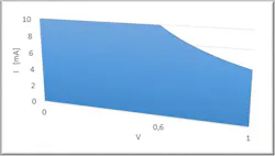
Another specific requirement for these type of products is to limit the power applied during test (Figure 3). Even when performing only power-off in-circuit tests on the components of the board, quality and reliability rules impose the constraints that injected voltage, current, and power to be always limited. Selected tests include net-impedance and shorts tests, discrete in-circuit tests, capacitive tests for opens, and other complementary tests. To fulfill this requirement during test generation, debug, and execution, the Pilot V8 allows micro-code modifications to the DSP of its stimulus and measurement system, to limit, for example, voltage to 1 V, current to 10 mA, and maximum power to 6 mW. Finally, remembering that the cost of the boards to be tested for a satellite could be as high as the price of the test equipment, a number of test scenarios have been simulated to stress the test system reaction in case of power failures or other unexpected events to assure that the test sequence is safely interrupted without any damage to the board under test.
Pilot V8 is now deployed with different manufacturers for such products. On the first installation, with active customer cooperation, tests and verifications were run for over two months, with boards being accurately verified after each sequence of tests, until the solution was officially approved. A special frame has also been designed to properly host the boards that have unusual form and size, assuring precise positioning on the tester. Having gained confidence on the solution, users have subsequently upgraded the system capabilities to power-up the board under test and run thorough functional tests, taking full advantage of the extended access enabled by the flying probe.
About the Author

Rick Nelson
Contributing Editor
Rick is currently Contributing Technical Editor. He was Executive Editor for EE in 2011-2018. Previously he served on several publications, including EDN and Vision Systems Design, and has received awards for signed editorials from the American Society of Business Publication Editors. He began as a design engineer at General Electric and Litton Industries and earned a BSEE degree from Penn State.
Voice Your Opinion!
To join the conversation, and become an exclusive member of Electronic Design, create an account today!

Leaders relevant to this article:


