Metadevices Tackle the Terahertz Gap
What you’ll learn:
- Why scaling down reaches a limit in the terahertz range.
- How metastructures change the approach to building components for THz frequencies.
- The researchers’ approach and results for these metastructures.
The terahertz swath of the electromagnetic spectrum presents a conundrum. On one side, it offers so much potential bandwidth and the associated benefits, as well as some unique propagation idiosyncrasies. On the other side, it’s too high in frequency for most electronic components and interconnects as we have them today, yet too low to function effectively with optical-class devices and configurations.
Furthermore, the traditional path of extending to higher frequencies via shrinkage may be reaching an atomic-level limit. Among other issues, the carrier injection through tunneling junctions dominates the channel resistance, while the high parasitic capacitances drastically limit the maximum operating frequency.
In addition, these ultra-scaled devices can only operate to a few volts due to the extremely high electric fields, which limits their maximum deliverable power. Thus, the terahertz region is an attractive region that can be seen but not yet accessed.
This dilemma hasn’t stopped researchers from trying to work in that band and develop suitable components and techniques; in fact, it’s an attractive challenge to many of them. For example, a team at Switzerland’s prestigious School of Engineering of their École Polytechnique Fédérale de Lausanne—EFPL (also known as the Swiss Federal Institute of Technology)—has analyzed, designed, and tested a new approach to electronics that could overcome these limitations.
Rearranged Device
Instead of shrinking the device, they rearranged it, primarily by etching patterned contacts called metastructures at sub-wavelength distances onto a semiconductor substrate made of gallium nitride and indium gallium nitride (Fig. 1). Crucially, the device can operate at electromagnetic frequencies in the terahertz range between 0.3 and 30 THz (that’s 300 to 30,000 GHz).
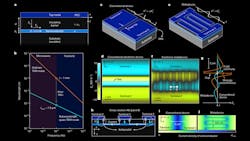
1. Concept of electronic metadevices based on the microscopic manipulation of RF fields leading to extraordinary electrical properties: (a) Schematic of a thin structure. (b) Wavelength versus frequency of an ordinary TEM mode, as well as the subwavelength quasi-TEM mode (d = 10 nm). (c) Illustration of a structure with a discontinuity on the top metal. The excited subwavelength mode results in oscillatory fields close to the gap. (d) Simulated Ez (real part) at the barrier of an 8-nm, thin structure with 100-nm long gaps at 120 GHz. (e) Metadevice geometry on the same structure; instead of a straight gap, stripes with a subwavelength length are patterned to form metastructures. (f) Simulated Ez at the barrier of a metadevice with 100-nm long gaps at 120 GHz. (g) Simulated Ez at the barrier along the propagation axis (x) for a straight-gap (conventional) device (blue) and metadevice (red). (h) Illustration of the electric field at the barrier for a metadevice (in f). (i,j) Simulated semiconductor current density for the straight-gap device (i) and the metadevice (j), showing a greater current confinement for the metadevice.
In these metadevices, the microscopic manipulation of RF fields results in extraordinary electronic properties. The devices operate on the basis of electrostatic control of collective electromagnetic interactions at deep subwavelength scales, as an alternative to controlling the flow of electrons in traditional devices, such as diodes and transistors.
This enables a new class of electronic devices with cutoff frequency figure-of-merit well beyond 10 THz, record high conductance values, extremely high breakdown voltages, and picosecond switching speeds (Fig. 2). These metastructures enable the electrical fields inside the device to be controlled, yielding special properties that don’t occur in nature.
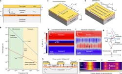
2. (a) Micrograph of a fabricated three-terminal metadevice. One terminal is pumped with a radio-frequency signal and the state of the device is controlled by the gate terminal. In an integrated-circuit form factor, the gate terminal of the metadevice can be controlled similarly to a field-effect transistor, by either applying an over-threshold bias (OFF state) or by floating the terminal (ON state). (b) Simulated electric-field pattern (real part) at the barrier for a gated metadevice in the ON state showing that the gate doesn’t perturb the electric-field pattern. (c) Simulated electric-field pattern (real part) at the barrier for a gated metadevice in the OFF state, in which the gate electrode depletes the 2DEG underneath it. (d) Measured output signal of the gated metadevice showing sub-10-ps switching.
While the most advanced devices on the market today can achieve frequencies of up to 2 THz, their metadevices had a cutoff figure of merit (FOM) beyond 10 THz and reaching 20 THz, high conductance values, and picosecond switching speeds (Fig. 3). In addition, while today’s devices operating near the terahertz range tend to break down at voltages below 2 V, the metadevices can support over 20 V.
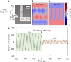
3. High-frequency characterization of electronic metadevices: (a) Schematic of the experimental setup to characterize electronic metadevices based on complex scattering parameters. (b) Photograph of the setup corresponding to the 0.75- to 1.1-THz band. (c) Measured ON-state resistance (RON) and OFF-state reactance (XOFF) of a terahertz metadevice with eight stripes (1.7 µm × 330 nm) and channel length of 120 nm (inset) versus frequency. (d) Benchmark of metadevices against mainstream electron devices on a COFF–RON plane, showing an outstandingly high cutoff frequency figure of merit (FOM) for electronic metadevices. Dashed lines represent the impedance of a 3.8-Ω resistance and a 2.3-fF capacitance. Electronic metadevices can achieve RON values below 10 Ω at very high frequencies, corresponding to insertion losses below 1 dB.
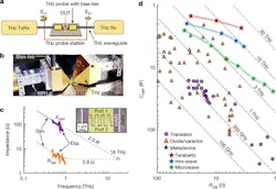
They also demonstrated and measured a metadevice-based modulator that shows impressive interchannel performance at 0.52 THz (520 GHz) (Fig. 4).
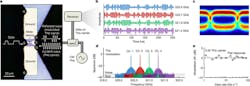
4. High-performance THz data transmitters using electronic metadevices: (a) Optical microscope image of an electronic metadevice modulator. The data signal, fed into the left port, modulates the incident THz continuous wave (CW) injected in the right port. The reflected wave is the data signal on the THz carrier, which is received by a coherent receiver. (b) Received modulated signals with four different carrier frequencies. The very high ON/OFF ratio shows that metadevice modulators are operational at frequencies much above 0.5 THz. (c) Eye diagram of the 520.4-GHz channel indicating an excellent modulation. (d) Spectrum of the received signals. The high-performance modulation results in almost zero crosstalk between channels, which indicates the potential of metadevice modulators for ultra-dense allocation of channels in massive communication networks. (e) The modulation efficiency (normalized to that obtained at 100 MHz) versus data rate, indicating an efficient modulation of THz signals with very high data rates.
The work is detailed in their paper with the brief title “Electronic metadevices for terahertz applications” published in Nature. The appended “Extended Information File” contains eight more figures and captions, as well as tables providing their metadevice dimensions along with a chart “Comparison of terahertz switches realized based on metadevice concept with classic devices.” The chart lists key parameters of their device versus the same parameters for representative FETs, Schottky diodes, PIN diodes, MEMS devices, memristors, and phase-change devices.
References
IEEE Spectrum, “Wireless Industry’s Newest Gambit: Terahertz Communication Bands”
IEEE Spectrum, “Terahertz Waves Could Push 5G to 6G”
IEEE Spectrum, “The Truth About Terahertz”
About the Author

Bill Schweber
Contributing Editor
Bill Schweber is an electronics engineer who has written three textbooks on electronic communications systems, as well as hundreds of technical articles, opinion columns, and product features. In past roles, he worked as a technical website manager for multiple topic-specific sites for EE Times, as well as both the Executive Editor and Analog Editor at EDN.
At Analog Devices Inc., Bill was in marketing communications (public relations). As a result, he has been on both sides of the technical PR function, presenting company products, stories, and messages to the media and also as the recipient of these.
Prior to the MarCom role at Analog, Bill was associate editor of their respected technical journal and worked in their product marketing and applications engineering groups. Before those roles, he was at Instron Corp., doing hands-on analog- and power-circuit design and systems integration for materials-testing machine controls.
Bill has an MSEE (Univ. of Mass) and BSEE (Columbia Univ.), is a Registered Professional Engineer, and holds an Advanced Class amateur radio license. He has also planned, written, and presented online courses on a variety of engineering topics, including MOSFET basics, ADC selection, and driving LEDs.
Comment About the Article
To join the conversation, and become an exclusive member of Electronic Design, create an account today!

Leaders relevant to this article: