How to Manage the PCIe 5.0 Channel Insertion Loss Budget

Members can download this article in PDF format.
What you’ll learn:
- How PCIe 5.0 technology’s higher speeds introduce new design challenges.
- How the introduction of precoding in the PCIe 5.0 protocol enhances the robustness of the link.
- How retimers enable reach extension.
PCI Express (PCIe) technology is the most important high-speed serial bus in servers. Due to its high-bandwidth and low-latency characteristics, PCIe architecture is widely used in various server interconnect scenarios, such as:
- Within a server: CPU to GPU, CPU to network interface card (NIC), CPU to accelerator, CPU to SSD
- Within a rack: CPU to JBOG and JBOF through board-to-board connector or cable
- Emerging GPU-to-GPU or accelerator-to-accelerator interconnects
At the same time, with the rapid development of heterogeneous computing, the data-throughput requirements in the server system are becoming increasingly higher. Two years after the release of the PCIe 4.0 Base Specification, the PCIe 5.0 Base Specification was officially released in May 2019 to address these requirements.
PCIe 5.0 technology still uses the same 128b/130b coding scheme, while the symbol rate increased from 16 GT/s to 32 GT/s. In keeping with tradition, the PCIe 5.0 Base Specification is backwards compatible with lower-speed PCIe Base Specifications.
Addressing PCIe 5.0 Design Challenges
In the case of other standards greater than 30 GT/s, the PAM4 modulation method is usually used to make the signal's Nyquist frequency one-quarter of the data rate, at the cost of 9.5-dB signal-to-noise ratio (SNR).1
However, PCIe 5.0 architecture continues to use the non-return-to-zero (NRZ) signaling scheme. Thus, the Nyquist frequency of the signal is one-half of the data rate, which is 16 GHz. The higher the frequency, the greater the attenuation. Consequently, signal attenuation caused by the channel insertion loss (IL) is the biggest challenge of PCIe 5.0 technology system design.
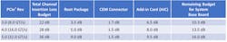
The PCIe 5.0 Base Specification outlines the bump-to-bump IL budget as 36 dB for 32 GT/s, and the bit error rate (BER) must be less than 10-12 (see table). To address the problem of high attenuation to the signal, the PCIe 5.0 Base Specification defines the reference receiver such that the continuous-time linear equalizer (CTLE) model includes an ADC (adjustable DC gain) as low as −15 dB, whereas the reference receiver for 16 GT/s is only −12 dB. The reference decision feedback equalizer (DFE) model includes three taps for 32 GT/s and only two taps for 16 GT/s.
In addition, the possibility of errors on the serial link becomes higher as the data rate reaches 32 GT/s. Due to the significant role that the DFE circuit plays in the receiver’s overall equalization, burst errors are more likely to occur compared to 16 GT/s.
To counteract this risk, PCIe 5.0 architecture introduces precoding in the protocol. After enabling precoding at the transmitter side and decoding at the receiver side, the chance of burst errors is greatly reduced, thereby enhancing the robustness of the PCIe 5.0 Base Specification 32 GT/s Link.
Deep Dive into PCIe 5.0 Channel Insertion Loss Budget
Here, we analyze the loss budget from the system base-board design and the post-equalized signal inside the SerDes receiver of the link, respectively.
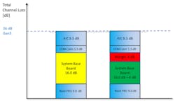
When looking at the 16-dB system base-board budget, engineers need to consider the following factors:
- As the PCB temperature or humidity rises, the IL of the PCB trace becomes higher.
- Process fluctuation during PCB manufacturing can result in slightly narrower or wider line widths, which can lead to fluctuations in IL.
- The amplitude of the Nyquist frequency signal (16-GHz sine wave in the case of 32-GT/s NRZ signaling) at the source side is 800 mV p-p, which will reduce to about 12.7 mV after 36 dB of attenuation. This underscores the need to leave some IL margin for the receiver to account for reflections, crosstalk, and power-supply noise that all potentially will degrade the SNR.
Thus, the IL budget reserved for the PCB trace on the system base board should be 16 dB minus some amount of margin (Fig. 1), which is reserved for the above factors. In summary, the 16 dB should be considered as the worst-case scenario on the system base board.
Now let’s analyze the loss budget from the aspect of the post-equalized signal inside the SerDes receiver of one link.
As a system engineer designs the system, it’s necessary to manage the passive channel topology so that the worst-case insertion loss of the link is less than 36 dB. Also, targeting lower BER than 1E-12 will lead to a wider open post-equalized eye, thus leaving more margin for a SerDes receiver to work.
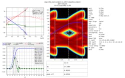
The Seasim 1.0.6 simulation tool is used here to simulate the eye height of a post-equalized signal inside the reference receiver. By adjusting the insertion loss of the channel, simulations targeted at different BERs were done. As expected, the smaller the insertion loss, the higher eye height can be achieved across different BER targets (Fig. 2).
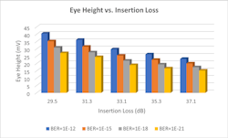
For example, for the case of 29.5 dB@BER 1E-21, the eye height is 27.19 mV (Fig. 3), while for the case of 37.1 dB@BER 1E-21, the eye height is only 15.3 mV.
The above Seasim simulations were done with ideal channels. The real channels could be much more challenging; thus, lower eye-height numbers are expected from Seasim simulations. In addition, further analysis like bit-by bit simulations and real measurements are needed to make a conclusive decision.
In any case, it will be reasonable to leave 10%-20% of the overall channel IL budget as margin to obtain a lower BER than 1E-12 and achieve a wider open eye for the post-equalized signal inside the SerDes receiver. In the case of a 36-dB budget, this amounts to 4 to 7 dB.
Advanced PCB Materials and Retimers: Keys to Success
As the demand increases for artificial intelligence and machine learning, PCIe 5.0 technology will enable more system topologies. The change from PCIe 4.0 architecture to PCIe 5.0 architecture brings the channel IL budget from 28 dB to 36 dB, which will create new design challenges. By leveraging advanced PCB materials to ensure sufficient end-to-end design margin, system designers can ensure a smooth upgrade to PCIe 5.0 architecture.
Also, a PCIe 5.0 retimer should be able to provide up to 36 dB reach extension. This means adding one retimer will allow one PCIe 5.0 link to operate up to 72 dB. What’s more, it’s possible to cascade up to two retimers per the Specification. With retimers, it’s safe to say that system designers could design even more complex systems with reasonable margin reserved on each segment of the PCIe 5.0 link.
References
1. "AN 835; PAM4 Signaling Fundamentals," [Online]. Available: https://www.intel.com/content/dam/www/programmable/us/en/pdfs/literature/an/an835.pdf.
2. PCI-SIG, "PCI Express Base Specification Revision 5.0 Version 1.0, 2019," [Online]. Available: https://pcisig.com/.
3. PCI-SIG, "PCI Express Card Electromechanical Electromechanical Revision 5.0, Version 1.0, 2021," [Online]. Available: https://pcisig.com/.
About the Author
Liang Liu
Systems and Applications Engineer, Astera Labs – PCI-SIG Member
Liang Liu is a Member of Technical Staff at Astera Labs. He has more than 15 years of high-speed interface product experience, including system design, application support, and product definition. He enjoys addressing the signal-integrity challenges on various high-speed interfaces using Astera Labs’ retimers.
Comment About the Article
To join the conversation, and become an exclusive member of Electronic Design, create an account today!

Leaders relevant to this article: