RF Module Brings It All Together for the Wireless IoT
What you'll learn:
- Reducing RF tradeoffs in the wireless IoT landscape.
- The monolithic integration for RF modules.
- Features of pSemi's PE562212 front-end module.
Multiprotocol wireless SoCs handle most of the heavy lifting in today’s IoT devices. Still, the final stretch of the RF signal path — those last several inches to the antenna — can be critical. Bridging this gap is the RF front-end module (FEM).
While companies are integrating power amplifiers (PAs), low-noise amplifiers (LNAs), and switches (SW) directly into their IoT SoCs, a separate FEM can be used to extend range and connection robustness in noisy RF environments.
“Unlike integrated PAs or RF front ends found on SoCs, external FEMs deliver superior performance,” said Xinliang Wang, senior director of product portfolio management at pSemi. “This is achieved through higher output power, enhanced receive sensitivity, and greater flexibility in power control.”
However, it tends to be a challenge to cram all of the different building blocks of the FEM – notably the PA, LNA, and SW – into a single module that works within the context of a low-cost, space-constrained IoT device.
As engineers grapple with the tightening cost and space constraints of the IoT, pSemi tries to bring these components closer together with its RF silicon-on-insulator (SOI) technology. Using what the company calls its UltraCMOS technology, it can integrate the main parts of the FEM into a single monolithic unit that saves space while competing with other RF technologies in terms of power amplifier output and receiver sensitivity.
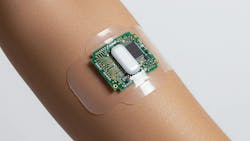
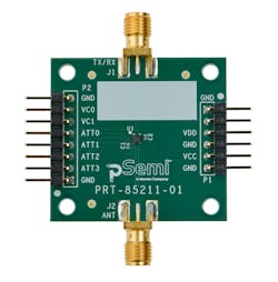
The UltraCMOS technology underpins its most compact RF FEM to integrate the PA, LNA, and SW into a single module — the PE562212. The 2.4-GHz FEM features very low noise that enables extended wireless range. It connects everything from smart speakers, smart lighting, smart thermostats, and other home appliances to wireless audio and medical wearables to sensors embedded on factory floors to ensure link robustness.
The multiprotocol FEM supports Bluetooth and Bluetooth Low Energy (LE) for short-range communications, Zigbee and Thread for mesh networking, and low-to-medium throughput Wi-Fi, giving more flexibility to IoT device makers (Fig. 1).
Reducing RF Tradeoffs in the Wireless IoT Landscape
The reliability, range, and speed of wireless connectivity in IoT devices depends on RF front-end and the PA inside it, which directly impacts the robustness of the wireless connection and power consumed by the device.
In most cases, these power amplifiers are based on bulk CMOS technology and integrated directly into IoT SoCs. While these RF components can enable robust performance and range, they tend to be optimized for power efficiency above all. The output power of these PAs is also often limited by harmonic generation, which may reach the limits set by regulations and certifications, or by the tight requirements of battery-powered IoT devices.
Multiprotocol wireless SoCs are designed to deliver the best link budget for the power envelope. That’s largely determined by the receive sensitivity, but it’s also defined by how efficiently the RF transceiver in the SoC has been designed.
Integrating digital, analog, and RF functions on a single chip has its difficulties and often leads to tradeoffs. These include reducing transmit power and receiver sensitivity, or how frequently the wireless SoC transmits.
Wang said it can make sense to use a separate FEM to boost the link budget, making sure that signals are transmitted and received with maximum efficiency and minimal loss. In many cases, these modules rely on RF-focused process technologies, such as silicon germanium (SiGe) and gallium arsenide (GaAs), to boost power efficiency at the expense of tight integration.
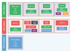
But that means traditional IoT FEM solutions are typically assembled in parts: Power amplifiers based on SiGe or GaAs to enable efficient, long-range transmission are frequently paired with separate LNAs and SWs based on RF-SOI, which is well-suited for faster switching and better signal reception, in a module (Fig. 2). Though it’s ideal for switching between different frequency bands or amplifying weak wireless signals, RF-SOI can have its limits when used in PAs.
pSemi claims to close the performance gap with its UltraCMOS technology. UltraCMOS is based on RF-SOI, which is widely used in the RF front ends crammed into 4G and 5G smartphones. However, the company said it brings improvements in power capacity, linearity, isolation, and switching performance (RON × COFF) on top of it by uniquely using a sapphire substrate.
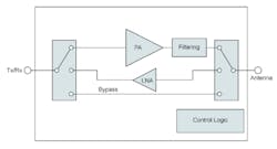
Using the monolithic integration made possible by CMOS, it can build the PAs, LNAs, and RF switches into a single IC, eliminating the mixing and matching of different RF blocks (Fig. 3).
“RF front ends in smartphones are highly complex and optimized for speed and high data rates across many cellular bands, while IoT devices prioritize simplified RF designs for extreme low-power, long-range, and protocol-specific communication,” said Wang. “Smartphones use advanced filtering and integration to manage interference from multiple radios, whereas IoT devices are more focused on power efficiency to maximize battery life.”
The Monolithic Integration for RF Modules
The high-performance PA at the heart of the PE562212 delivers up to +21-dBm output to improve signal transmission, while supporting application-specific output power requirements through 1-dB gain steps.
The IoT FEM also incorporates LNAs with a 1.6-dB noise figure to strengthen signal reception and RF switches designed for minimal loss. Furthermore, it features integrated RF filters to reduce harmonics and distortion as well as a bypass path with 0.6-dB loss. The combination of high output power and low noise provides a robust link budget, which is critical for penetrating walls and ensuring extended range and reliability, according to the company.
pSemi said the PE562212 has the ability to support the most widely used wireless protocols in the IoT. For instance, it can be used in a smart-home device that uses Bluetooth LE to connect to a smartphone while it downloads firmware updates over Wi-Fi at the same time. That tends to require more linearity than what’s possible with a wireless SoC alone.
“For IoT devices, especially wearables and smart sensors, maintaining robust RF performance is a key design challenge given their increasingly compact size,” said Wang.
While it reduces excessive packet drops and power consumption by increasing link budget, the RF FEM has robustness against ESD and ruggedness to handle the harsh environmental conditions inherent to the IoT.
The new module comes in a compact 1.8- ×1.8- × 0.63-mm LGA package suited for space-constrained applications. It enables easier PCB design with I/O interfaces requiring no external matching, said pSemi.
About the Author

James Morra
Senior Editor
James Morra is the senior editor for Electronic Design, covering the semiconductor industry and new technology trends, with a focus on power electronics and power management. He also reports on the business behind electrical engineering, including the electronics supply chain. He joined Electronic Design in 2015 and is based in Chicago, Illinois.
Comment About the Article
To join the conversation, and become an exclusive member of Electronic Design, create an account today!

Leaders relevant to this article: