Hard-Won Knowledge Mitigates Effects Of Tin Whiskers

July 1, 2014 will mark the eighth anniversary of the European Union’s Restrictions on Hazardous Substances (RoHS) directive. When it was enacted, the industry knew that the elimination of lead from electronic products would lead to “tin whisker” problems. Since then, the industry has learned a lot about mitigating their effects.
This file type includes high resolution graphics and schematics when applicable.
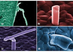
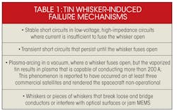
Tin whiskers are slim metallic filaments that emanate from the surface of tin platings (see the figure). These filaments are conductive and can cause shorts across adjacent conductors—and these shorts can cause some really bad failures (Table 1). But with all of this knowledge, the industry is still struggling with how to predict and prevent these “needles of pain.”
Companies may avoid some potential issues by conducting a continuous and consistent effort to maintain as many possible sources of high-reliability components as possible. To do this, they must first find out if their suppliers intend to switch to pure tin electroplating or lead-free soldering. Those who indicate such intent should be provided with information intended to convince them to either reconsider switching or to maintain the capability to produce high-reliability components in parallel with lead-free components.
The uncertainties associated with tin whisker growth make it extremely difficult to predict if or when tin whiskers may appear. There are currently no industry-accepted accelerated test methods to judge a particular product’s propensity to form whiskers. Due to the difficulties in predicting tin whisker growth, it may not be possible to completely eliminate tin whiskers as a failure risk.
Fortunately, various mitigation techniques are available. They include tin alloys, solder dip, conformal coatings, under-plating, annealing, strip and re-plate terminations, and conductor spacing/application specific mitigation.
Tin Alloys
Utilization of procurement specifications that have clear restrictions against the use of pure tin plating is highly recommended. Most of the commonly used military specifications currently have prohibitions against pure tin plating. Studies have shown that alloying tin with a second metal reduces the propensity for whisker growth.
Alloys of tin and lead are generally considered to be acceptable where the alloy contains a minimum of 3% lead by weight. Although some experimenters have reported whisker growth from tin-lead (SnPb) alloys, such whiskers have also been reported to be dramatically smaller than those from pure tin plated surfaces and are believed to be small enough to not pose a significant risk for the geometries of today’s microelectronics.
It can be dangerous to rely on the part manufacturer’s certification that pure tin plating was not used in the production of the product supplied. Studies have shown at several instances where the procurement specification required “no pure tin,” but the product supplied was later determined to be pure tin. In some of these instances, tin whisker growths were also discovered. Users are advised to analyze the plating composition of the products received as an independent verification.
Solder Dip
When pure tin plating cannot be avoided, other mitigations must be investigated. One such mitigation is the solder dip of lead-free component finishes with SnPb.
A SnPb solder dip process may be used to recoat the component leads. Solder of 63/37 or 60/40 can be used. Precautions are required to prevent damage to the parts. Possible damage can include package cracking or loss of hermeticity resulting from thermal shock, popcorning of plastic packages, solder bridging between leads on fine-pitch packages, solder bridging between leads and the component body, and handling damage such as bent or non-coplanar leads and electrostatic discharge.
The success of solder dipping as a tin whisker risk-mitigation approach depends on coating the entire exposed tin plated surface. If portions of the tin are left uncovered by the SnPb solder, they can still grow whiskers. With the exception of robust through-hole parts, all components must be dipped in accordance with GEIA-STD-0006.
A specialist sub-contractor compliant with these requirements will perform the operation using an automated robot system. Larger, more robust parts for axial or radial leaded parts, for example, can be dipped by hand and in house by the printed-circuit board (PCB) assembler.
Conformal Coating
Just as the name implies, conformal coating is a coating with an inert material that can protect electronic circuit boards from the problems related to tin whisker growth: shorts, plasma arc, and debris. Four points should be considered while using conformal coating as a tin whisker mitigation technique:
• It must slow the formation of tin whiskers. We acknowledge that tin whiskers cannot be stopped until we understand how they form in the first place.
• It must prevent the outward escape of any tin whiskers that do nucleate.
• It must prevent the penetration of whiskers formed outside the conformal coat.
• It must protect the coated circuit board from loose whisker debris.
Boeing, Schlumberger, Lockheed, Raytheon, the National Physical Laboratory (U.K.), the Center for Advanced Life Cycle Engineering (CALCE), NASA, and other organizations have studied many types of conformal coatings over the years (Table 2).
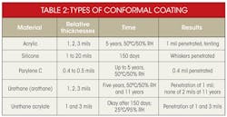
No conformal coating meets all these criteria. However, the Arathane coating seems promising when applied sufficiently thick, and the conformal coating does prevent shorts from debris. Ultimately, no coating is 100% effective, and whiskers still grow. Thermal effects need to be considered if a conformal coating is used on parts that will need to dissipate heat when operating. If necessary, the device may need to be derated.
If the conformal coating fails to contain whisker formation, the effectiveness of a conformal coat in providing protection against electrical leakage and corrosion will be compromised. A puncture site may provide an increased opportunity for excessive leakage currents that can produce transient or permanent failures.
Another concern related to whisker formation is the potential for whiskers to produce minor de-lamination of the conformal coating from the circuit board. The resulting capillary space could provide a void for condensation of the water vapor molecules that slowly diffuse through the coating material. This creates the slim possibility of galvanic corrosion, though it may not be of consequence.
Further, emerged whiskers that break loose may end up in other areas of your hardware that are vulnerable to conductive debris. However, this risk is substantially reduced compared to the scenario of not using a conformal coat.
Under-Plating/Inter-Metallic Formation
The formation of intermetallics in the base metal below the pure tin plating may create stresses that promote the growth of tin whiskers. Based on this assumption, a barrier layer such as nickel between the base metal and the pure tin finish may reduce the likelihood of tin whisker growth. One study indicates that tin whiskers can grow on parts with nickel under-plating. In another study, a nickel barrier layer of 1.5 µm over a copper base material significantly reduced the growth of tin whiskers on a low-stress tin finish.
Thin plating (less than 1 µm) or thicker plating (greater than 20 µm) may reduce the tin whisker formation. Unfortunately, the thin plating may reduce the ability of the finish to serve other necessary functions such as resisting corrosion. But while higher thickness may reduce internal stress in the plate, mechanical damage and/or long-term growth of intermetallics may still initiate whisker formation.
Annealing
Annealing after plating has become a widely accepted whisker mitigation technique. Annealing at 150°C for one hour within one hour of plating is an acceptable mitigation technique as long as the part is also conformal coated after soldering to the board. Annealing has been proved to reduce the maximum whisker length and the growth rate by relieving plating stresses, causing grain growth and increasing grain sizes while also forming a uniform inter-metallic layer of Cu6Sn5 over Cu3Sn, which slows further inter-metallic growth.
For semiconductor parts, surface finishes are subjected to various forms of annealing, such as cure bakes and burn-ins. These processes may have mitigated whisker formation on existing SnPb finishes.
While evidence of removal of compressive residual stress has been shown to significantly reduce the onset of tin whisker formation, it is not clear that whiskers will not be an issue in 10 to 30 years. Mechanical damage and other factors may induce compressive stresses sufficient to initiate whisker growth.
Strip & Re-Plate Terminations
If alternatives to tin plated parts cannot be obtained, it may be possible to remove the tin finish. This is normally risky on electronic components. The ability to remove the tin plating from the affected surfaces and refinish these surfaces must be made after a risk and cost analysis.
Such processes should be reviewed to determine the potential for affecting the reliability of the original product (e.g., a chemical attack on component materials). This method is not approved and should be carefully reviewed prior to any use, as it is perceived to be very risky.
Conductor Spacing/Application-Specific Risks
In terms of application-specific considerations, the proximately of adjacent conductors is a particular concern. For example, a 0.5-mm pitch, 208-pin plastic quad flat-pack (PQFP) package can have spacing between adjacent leads as small as 230 µm, and the spacing between adjacent pads can be as small as 100 µm.
For some high-density applications, the spacing between conductors has been reported as small as 76 µm. Design rules normally call for 530-µm spacing between external conductors and 500 µm between internal conductors. Whisker growth of 250 µm can easily create shorts in high-density applications. Growths above 1 mm (1000 µm) can induce shorts under current design rules.
To remove the threat of shorts due to tin whiskers, engineers should review the criticality of the system or subsystem as well as its desired life expectancy. As presented above, a variety of application-specific considerations may be used to assess the risk of whisker-induced failures and assist in making “use as-is” or “repair/replace” decisions.
These factors include circuit geometries that are sufficiently large to preclude the risk of a tin whisker short, mission criticality, mission duration, collateral risk of rework, schedule, and cost. At present, any pure tin finished surface can be considered as having the potential to grow tin whiskers.
Tin whisker mitigation strategies are recommended due to the whisker growth phenomenon associated with tin during the soldering process. Cypress Semiconductor has acknowledged the problem and minimized it by adding lead to the soldering process.
Even with many studies and experiments performed globally on tin whisker growth, there is still no definite conclusion on how or why tin whiskers form. An established method performed at Cypress to relieve the stress of tin plating added annealing or post-bake during the solder plate process with one-hour, 150°C condition. This is adequate to confirm that growth is significantly reduced, but appropriate prevention and a suitable solution for tin whisker growth are still unresolved and unknown.
For health and environmental reasons, lead was identified as a hazardous substance, and the soldering process is now lead-free. To maintain the reliability and quality of Cypress products, the company implemented its Tin Whisker Mitigation Program on all pure tin products.
References
1. NASA’s research on tin whiskers: http://nepp.nasa.gov/whisker./background/index.htm
2. “Whisker (metallurgy),” Wikipedia, http://en.wikipedia.org/wiki/Whisker_(metallurgy)
3. CALCE, www.calce.umd.edu/tin-whiskers/
Abhishek Gupta is a business analyst for Cypress Semiconductor. He has a BE in electronics & communications from Maharishi Dayanand University, Haryana, India. He has worked with Agilent Technologies as a logistics coordinator (RoHS specialist). He can be reached at [email protected].
About the Author
Abhishek Gupta
Abhishek Gupta is a business analyst for Cypress Semiconductor. He has a B.E. in Electronics & Communications from Maharishi Dayanand University, Haryana, India. He has worked with Agilent Technologies as a Logistics Coordinator (RoHS Specialist).
Comment About the Article
To join the conversation, and become an exclusive member of Electronic Design, create an account today!

Leaders relevant to this article: