Calculating Essential Charge-Pump Parameters
Capacitive charge-pump circuits are used in many applications. And though these circuits appear deceptively simple, engineers working on them need a thorough understanding of how they function. By analyzing the model of a basic charge-pump circuit, it's possible to derive expressions for efficiency and output voltage as functions of the pump's duty cycle, switching frequency, output and flying capacitances, switch and other series resistances, and load.
The model derived in this article enables designers to understand and predict the behavior of charge pumps under a wide variety of conditions. Mathematical derivations are shown in the PDF version of this article to provide a full understanding of the model and to provide a general approach for analyzing other complex power-supply circuits.
Developing the charge-pump model requires some lengthy derivations of key equations. For the complete derivations in their entirety, click here. There is also a spreadsheet that automates the final expressions derived here, allowing a quick calculation of essential charge-pump parameters including output voltage and efficiency.
Charge pumps use a charge-storage element (i.e. a capacitor) to transfer charge from a source to a load. Fig. 1 shows the basic model of a charge pump. It can represent several topologies, such as regulated stepdown charge pumps, inverting regulated charge pumps and inverting unregulated charge pumps. For inverting charge pumps, the output voltage is negative, but the magnitude of that voltage is the same as that predicted by the model. Stepup or boost charge pumps operate in a very similar fashion; however, there are a number of key differences that are not taken into account in the model described in this article. Thus, the model cannot readily be applied to describe their operation.
For unregulated charge pumps, R1 represents the total resistance of the internal switches, which are usually MOSFETs. For regulated charge pumps, the resistor R1 is a variable resistance that can be implemented by varying the bias of the MOSFET switch in the on state.
This resistor regulates the charge pump's output voltage. Unlike inductive dc-dc converters, in which the output voltage is regulated according to the duty cycle of the switch, output voltage for the charge pump is regulated by changing the value of this resistance.
The switch is controlled by an oscillator that alternates between position 1 and position 2 (Fig. 1). We assume for this analysis that the circuit is operating in the steady-state mode. That is the condition used to derive an expression for output voltage as a function of all the variables.
Interval One
Because of the steady-state assumption, each capacitor will be charged to some initial voltage. We can provide those voltages by placing an initial condition on each capacitor (i.e., a voltage source connected in series with the respective capacitor), which we will call V1 and V2. The resulting circuit is shown in Fig. 2.
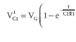
Having established the initial conditions, let's solve for the two capacitor voltages during the first interval (I), when the switch is connected to position 1. (For interval two [II], the switch is in position 2.) The voltage across C2 is always the output voltage of the charge pump. Solving for the voltage across C1 during interval one, i.e., VIC1 (t), we obtain the following expressions:
Eq. 1 gives an expression for voltage across the flying capacitor (C1) during interval one. Note that this voltage is a function not only of the element values, but also of the initial condition V1. By inspection, the output voltage VIC2 (t) across output capacitor C2 during interval one is:
Interval Two
Next, we evaluate what happens when the switch flips to position 2. It goes to position 2 at t=DT, where D is the duty cycle of the switching frequency and T is its period. Since we evaluate this interval separately, we must set the appropriate initial conditions for the two capacitors. We can call these initial conditions V3 and V4, but they are actually the final states of the capacitors at the end of interval one, and therefore can be derived from the expressions obtained in Eqs. 1 and 2. These conditions are shown in the schematic of Fig. 3.
Before analyzing the circuit in Fig. 3, we need the initial conditions V3 and V4. They can be obtained by recognizing that V3 is the voltage across C1 at time t = DT, and V4 is the voltage across C2 at t=DT. Therefore, we write the following expressions:
Having obtained the initial conditions for interval two, we can find an expression for voltages across the flying and output capacitors as we did for the first interval. To preserve clarity, we refer to the initial conditions in this interval as V3 and V4, even though they are actually functions of the initial conditions at interval one. Solving for the voltage across output capacitor C2 (VIIC2), we obtain the following equation (see derivations 1, 2 and 3 online):
where s1, s2, A′, B′, C′, and D′are constants that depend on the values of C1, C2, R1, and R2. Because the equations for these constants are rather complex and require a lot of space, they are presented in an appendix at the end of the online version of this article. (See Eqs. A1 through A6 in the appendix.)
The voltage across the flying capacitor during interval two is expressed as a function of the output voltage during that period, and simplified as follows (see derivations 4 and 5):
As for Eq. 5, the terms N2 and N4 are constants that depend on the values of C1, C2, R1 and R2. Because of the complexity of these equations, they are presented in the online appendix. (See Eqs. A7, A8, A9 and A10 in the appendix.)
Unifying Initial and Final Conditions
So far, we have equations that describe the voltages across the two capacitors in each of the intervals. Next, we need to equate the initial and final conditions in a way that forces the equations to represent steady-state operation.
To discuss this point further, we first examine the voltage across the output capacitor, which is the output voltage of the charge pump. During interval one, the output capacitor is connected to the load by itself, and its voltage drops from the initial condition V2. During that interval, the flying capacitor charges to a voltage higher than its initial condition V1. During the second interval, the flying capacitor connects to the output capacitor through R1, so the output voltage begins to increase.
For the system to be in equilibrium, note that the average output voltage has to be constant. The only way to achieve that condition is for the output voltage at the end of interval two to equal its initial voltage at the beginning of interval one. The same consideration applies to the conditions for the flying capacitor, because the average charge supplied to the output must be constant. We can write these two conditions in the following way:
Since is a function of V1 and V2, and is also a function of V1 and V2, we can form a system of two equations in two unknowns (V1 and V2), and solve for the equilibrium (steady-state) initial conditions for interval one. When we obtain V1 and V2, we can solve for every other parameter of interest, including the average output voltage, efficiency and output ripple, as a function of capacitor size, duty cycle, switching frequency, series resistance and load.
We now write and solve the system of equations. Eqs. 10 and 14 reduce to:
Plugging Eqs. 3 and 4 into Eqs. 15 and 16, and rearranging the terms slightly, we obtain the final system of two equations in the two unknowns V1 and V2:
To solve these equations, it is convenient to reduce their size by adopting a short notation for some of the constant terms.
We must also bear in mind that a final numerical solution is feasible only with a computer, which further justifies the change in notation. Making substitutions for all constant terms except V1 and V2, and rearranging them (see Eqs. A11 through A17 in the online appendix), we can rewrite the system of equations as follows:
We've now reduced the system of equations to a manageable form that can be solved for V1 and V2:
Eqs. 19 and 20 represent the result for which we have been working. They give the precise initial conditions for the charge-pump model in equilibrium, as a function of all of the parameters we specified at the beginning of this article: capacitor size, load, series resistance, frequency or period, and duty cycle. Knowing the values of V1 and V2, we can easily solve for other parameters of interest. Knowing V1 and V2 also allows us to plot waveforms for the capacitor voltages. Because the equations for V1 and V2 are rather complicated, we can use mathematical software such as Matlab or Excel to give precise numerical values and plot the results.
The latter part of this article presents several such plots, but first we derive some useful and important expressions. One such is the average output voltage.
Average Output Voltage
We find the average output voltage by integrating the output capacitor waveform over one period and dividing the result by the period interval T. Since this waveform consists of two separate waveforms for each interval, we can split the integral into two separate integrals as follows:
Evaluating the integrals, we obtain (see derivation 6):
Similarly, we obtain the average flying-capacitor voltage as follows:
Evaluating the integrals in Eq. 23, we obtain (see derivation 7):
Finally, we calculate the charge-pump circuit's efficiency. By definition, efficiency equals power delivered to the output divided by power consumed at the input. Since we have a device that is switching and whose voltage waveforms vary with time, we are interested in the ratio of the average power at input and output, as opposed to the ratio of instantaneous powers. We define the average power per period as the integral of instantaneous power divided by the period interval:
Evaluating the integrals in Eq. 26, we obtain (see derivation 8):
Next, we evaluate input power ¡ª the power that is delivered from the source VG to the charge pump. Note that input power is consumed only during the first interval, when the flying capacitor is connected. Because no constant load is connected to the input (or to the output), we can find the instantaneous input power by multiplying the input voltage VG by the input current. Thus, it can be shown that the instantaneous input power is:
Having obtained the average input power and average output power, we can now calculate the charge-pump efficiency as:
Applying the Results
So far, we've analyzed the operation of the charge-pump model presented at the beginning of this article. We obtained a number of equations that express circuit parameters in steady-state mode as a function of the capacitors used in the model, the series resistor with the flying capacitor, switching frequency, duty cycle, input voltage and load. These expressions were obtained by evaluating the circuit in each interval separately, and then forcing the initial-condition values in each interval to support steady-state operation in the circuit.
Many of the equations are complex, which hampers our intuitive understanding of how the circuit works. However, you can compensate for this drawback with mathematical software such as Matlab or Excel. With the expressions derived in this article, we can accurately simulate numerous scenarios by varying the circuit parameters, and thereby reveal a much more comprehensive picture of the circuit operation. You can add refinements to the simplified model presented previously, such as series inductances for the traces and series resistors for the capacitors. However, the subsequent analysis is fundamentally the same.
We can now plug the expressions obtained previously into our numerical-computation software and run some simulations to see how the circuit works. More importantly, we can discover whether our model predicts the operation of a real circuit with accuracy. A calculation spreadsheet in Excel allows you to input all circuit parameters discussed in this article, and obtain numerical values for the model's average output voltage and efficiency using the equations derived in this article.
We can now plug the expressions obtained previously into our numerical-computation software and run some simulations to see how the circuit works. More importantly, we can discover whether our model predicts the operation of a real circuit with accuracy. A calculation spreadsheet in Excel allows you to input all circuit parameters discussed in this article, and obtain numerical values for the model's average output voltage and efficiency using the equations derived in this article.
To test the validity of our model, a bench test was performed using a switched-capacitor voltage inverter from Maxim (MAX870). The internal structure of this device (an unregulated inverting charge pump) is close to that of the model, except the output voltage is inverted (i.e., the output ground connection is flipped during interval two). That action has no effect on the validity of the equations, but to compare with results from the model, we must ignore the output sign and consider only the absolute value of the output voltage.
A series of tests was performed in which the MAX870's load resistor (R2), flying capacitance (C1) and output capacitance (C2) were varied while measuring the absolute value of the output voltage. The results were then compared with those predicted by the calculation spreadsheet (Fig. 4, Fig. 5, and Fig. 6).
Other parameters for the circuit were measured experimentally: f = 134 kHz, D = 50% and R1 = 5 ¦¸. As can be seen, the experimental results agree very closely with results obtained using the MAX870, thereby validating the model as a convenient tool for quick calculations and first-order approximations when designing simple charge pumps.
Note that the charge pump's average output voltage is strongly influenced by the value of R1 (Fig. 7). Higher values of R1 cause the output voltage to drop in magnitude, and a proper choice of switching frequency, load and flying capacitor make the relationship nearly linear. This is important because it allows us to understand how to regulate the output voltage. The mechanism for regulation is almost analogous to that of a linear regulator.
For regulated charge pumps, R1 is a MOSFET whose resistance is regulated according to a feedback signal that senses the output voltage. You should obtain the range of values that R1 can assume from the data sheet for that particular charge pump. When working with unregulated charge pumps, on the other hand, R1 represents the sum of switch resistances seen by the flying capacitor.
That parameter, usually called internal switch resistance, should be specified in the data sheet for the charge-pump IC. Note that the capacitor may see more than one switch, in which case the resistance of individual switches should be added. If you include a flying capacitor with substantial series resistance, you should also account for that value in the parameter R1.
Finally, charge-pump efficiency is an important consideration. An increase of R1 causes efficiency to go down almost the same way as the output voltage. For relatively high switching frequencies, it can be shown that charge-pump efficiency is identical to that of an LDO (i.e., it equals the ratio of output voltage to input voltage).
Many other conclusions can be drawn from the model. To examine a parameter of interest while varying the input variables, be sure to use the calculation spreadsheet, appendix and derivations.
Comment About the Article
To join the conversation, and become an exclusive member of Electronic Design, create an account today!

Leaders relevant to this article: