Intel Foundry Open to the World

What you’ll learn:
- What is Intel Foundry?
- Why is Intel opening up its foundry?
- What kinds of technology will be provided by the Intel Foundry?
Intel now has a split personality. Its well-known processor, software, and logic technology is part of Intel Products, while its foundries are now part of Intel Foundry (Fig. 1). It has a church and state split, meaning the foundry will still make chips for its products as one of many customers rather than a dedicated foundry for Intel products as in the past.
Pat Gelsinger, Intel’s CEO, announced Intel Foundry at IFS Direct Connect 2024 in San Jose, Calif. All of the advanced chip and packaging technology will be available to Intel Foundry customers. Intel Foundry is already large to meet Intel’s product needs, but the new foundry plans on growth with a target of being the number two foundry by 2030.
The big kid on the block is Taiwan Semiconductor Manufacturing Company (TSMC). Other large foundries include GlobalFoundries and Samsung Foundry. Plus, many dedicated foundries for companies like Texas Instruments and Micron often target specific chip categories or product lines.
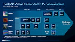
18A and 14A Nodes
The Intel Foundry will push the technology limits with its 18A and 14A nodes (Fig. 2). The 18A is 18-angstrom or 1.8-nm technology. The 18A naming convention is new and can be annotated with a P for a high-performance version and T for through-via stacking support. More mature nodes will receive this type of enhancement over time.
One aspect of the Intel Foundry stressed by Pat Gelsinger is that it’s not just a chip/wafer foundry, but rather a full stack solution that includes packaging technology, which has become extremely important. This includes the Embedded Multi-Die Interconnect Bridge (EMIB) used to provide chiplet support (Fig. 3).
EMIB is applied to Intel’s advanced FPGAs and other high-performance chips. It’s a combination of interposer and substrate. EMIB can provide hundreds to thousands of connections between a pair of chiplets, such as a processor and high bandwidth memory (HBM).
Foveros Facts
Foveros and Foveros Direct provide 3D die-to-die stacking support (Fig. 4). The initial Foveros was first used in 2019 in Intel’s Lakefield mobile processor. Intel's Ponte Vecchio GPU employs both EMIB and Foveros technology.
4. Foveros Direct provides 3D stacking support.
Foveros Omni is the third generation where Omni indicates an omnidirectional interconnect. Prior to this generation, the base die had to be larger than the top die. This generation supports through silicon vias (TSVs).
Foveros Direct is the fourth generation of Intel’s die-to-die connectivity. It utilizes direct copper-to-copper bonding instead of joining copper pillars using tin solder. The latter doesn’t scale well to small geometries. The die needs to be very flat for this to work. It improves the size of the interconnect bump density sixfold. TSMC provides a similar technology that it calls chip-on-wafer (CoW) or wafer-on-wafer (WoW).
Other technologies provided by Intel include its PowerVia that delivers power from the backside of the chip, leaving only logic connections on the top. A future technology involves glass substrates, which Intel has demonstrated (Fig. 5).
5. Intel’s glass substrate technology will be available at the Intel Foundry in the future.
All of the major EDA tool vendors, including Ansys, Cadence, Siemens, and Synopsys, were on hand to show their support. Intel also noted that it will receive funds from the U.S. Chips Act. The amount and its use haven’t been announced yet.
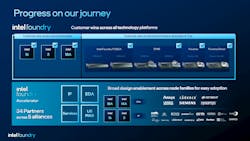
Intel Foundry is well-established and large, but opening it up is a significant change for both Intel and its customers. The need for more chip sources is being driven by general requirements, such as in the automotive sector, as well as the massive compute requirements of cloud artificial intelligence (AI) and edge AI. The company looks to address this growth as well as improve the chip and packaging technology.
About the Author

William G. Wong
Senior Content Director - Electronic Design and Microwaves & RF
I am Editor of Electronic Design focusing on embedded, software, and systems. As Senior Content Director, I also manage Microwaves & RF and I work with a great team of editors to provide engineers, programmers, developers and technical managers with interesting and useful articles and videos on a regular basis. Check out our free newsletters to see the latest content.
You can send press releases for new products for possible coverage on the website. I am also interested in receiving contributed articles for publishing on our website. Use our template and send to me along with a signed release form.
Check out my blog, AltEmbedded on Electronic Design, as well as his latest articles on this site that are listed below.
You can visit my social media via these links:
- AltEmbedded on Electronic Design
- Bill Wong on Facebook
- @AltEmbedded on Twitter
- Bill Wong on LinkedIn
I earned a Bachelor of Electrical Engineering at the Georgia Institute of Technology and a Masters in Computer Science from Rutgers University. I still do a bit of programming using everything from C and C++ to Rust and Ada/SPARK. I do a bit of PHP programming for Drupal websites. I have posted a few Drupal modules.
I still get a hand on software and electronic hardware. Some of this can be found on our Kit Close-Up video series. You can also see me on many of our TechXchange Talk videos. I am interested in a range of projects from robotics to artificial intelligence.
Comment About the Article
To join the conversation, and become an exclusive member of Electronic Design, create an account today!

Leaders relevant to this article: