Staying Current: Midyear 2025 EDA Tools for Engineers (Part 1)

What you'll learn:
- The latest in EDA tools across different practices.
- Who is leading in EDA tools?
- Where to begin with EDA tools.
The electronic design automation (EDA) space is evolving faster than most engineers can keep track of, with AI-driven optimizations, scalable cloud verification, statistical yield analysis, and silicon telemetry now baked into next-gen tools.
This roundup highlights just a few of the platforms that are changing front-end and back-end workflows, from RTL-to-GDSII closure to post-silicon diagnostics. These include tools used throughout product lifecycles and those specializing in AI for debugging and analysis.
Synopsys.ai Copilot for EDA

Synopsys has utilized LLMs for its Synopsys.ai Copilot, which is designed to boost the chip design process and productivity across all stages of chip design. The platform acts as an AI assistant that can answer questions, provide contextual recommendations, and even generate workflow scripts based on company requirements.
It also acts as an advanced knowledge query tool, garnering data from Synopsys manuals, application notes, videos, and its online SolvNetPlus community. As the Copilot learns from ongoing projects, it will enhance its guidance, including debug suggestions, optimization scripts, and design recommendations, thereby reducing tasks that traditionally take hours or days to just minutes.
Cadence Verisium Debug
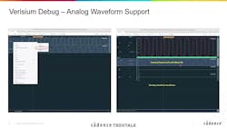
The Verisium Debug is an advanced, AI-powered debug solution for hardware and software design verification. It’s designed to boost the process of searching and fixing bugs in today’s SoCs and IPs. The platform integrates all of Cadence’s verification engines, including Xcelium Logic Simulator, Palladium emulation, and Protium, which provides a consistent debugging environment.
The Verisium Debug comes equipped with a range of apps meant to streamline the debugging process. They include Verisium AutoTriage (automated regression failure classification), SemanticDiff (ranking disruptive code changes), WaveMiner (identifying likely root cause signals in waveforms), PinDown (linking code changes to introduced bugs), Debug (AI-assisted multi-run debugging), and Manager (AI-driven test suite optimization and verification planning).
Siemens mPower Digital
Siemens’ mPower Digital power-integrity tool is designed for power-integrity analysis of analog, digital and mixed-signal ICs. It’s built on the Siemens Joint Enterprise Data and AI (JedAI) platform, which fully integrates with Cadence’s EDA tools and provides unified data management, deep analytics, and automated verification workflows. The platform offers an optimized graphical user interface (GUI) with features that include a waveform viewer, source-code browser, and SmartLog.
mPower Digital features Verisium waveform database technology (VWDB) for efficient waveform generation and supports various debugging requirements, including RTL, gate level, testbench, low power, mixed signal, embedded software, and more.
Cadence Cerebrus Intelligent Chip Explorer

Cadence’s Cerebrus Intelligent Chip Explorer, intended for digital full-flow implementation, takes advantage of reinforcement learning to optimize chip design in an automated fashion. According to the company, the platform isn’t just a simple ML recommendation tool; it’s a fully integrated AI engine that learns and iterates across design spaces to deliver improved power, performance, and area (PPA) metrics.
Engineers can guide the tool using design goals, and Cerebrus adapts its optimization over multiple blocks and configurations. It’s especially useful for SoC teams looking to scale workflows across increasingly complex design environments.
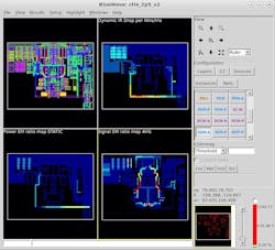
Ansys RedHawk-SC
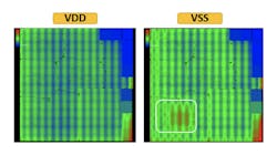
The RedHawk-SC from Ansys is a comprehensive EDA tool that performs power-integrity, thermal, and reliability analysis on complex SoCs. The platform allows engineers to analyze and mitigate power-related issues, including IR drop and electromigration (EM). It utilizes advanced power analytics (APA) and SigmaDVD technology to detect and correct dynamic voltage drop, which can impact performance and reliability.
RedHawk-SC’s features include IR-drop signoffs, thermal-aware EM analysis, timing impact of voltage variability, vector and vectorless activity, chip/package electrothermal co-simulation, cloud-native elastic compute, advanced root-cause, what-if, and ECO analyses.
proteanTecs Proteus

proteanTecs’ Proteus is a cloud-based analytics platform that leverages Universal Chip Telemetry (UCT) to provide insights into the health and performance of chips throughout their lifecycle, from design and production to field deployment. The platform utilizes embedded on-chip monitoring agents and machine learning to provide predictive maintenance, power optimization, and increased reliability for complex electronic systems.
While Proteus isn’t a traditional EDA tool, it does provide valuable insight into chip forensics. On-chip agents are embedded within the chip architecture during the design process and continuously gather real-time data on critical parameters, including voltage, temperature, timing margins, and interconnect quality.
The collected data is then processed and analyzed by Proteus' cloud-based analytics platform using advanced machine-learning algorithms and data-fusion techniques. That analysis provides insights and predictions into the chips' behavior under varying workloads and conditions, allowing for proactive identification and the mitigation of potential problems.
Conclusion
EDA in 2025 isn’t just about simulation speed or timing closure; it’s about building efficient, optimized designs with fewer bugs and increased predictability. The tools listed here are just a few of the platforms engineers can utilize to handle bigger chips, tighter nodes, and shorter schedules without signing off on quality. With that said, dig into the capabilities, and you’ll see why these platforms are redefining how silicon gets designed and verified today.
Stay tuned for Part 2.
About the Author

Cabe Atwell
Technology Editor, Electronic Design
Cabe is a Technology Editor for Electronic Design.
Engineer, Machinist, Cartoonist, Maker, Writer. A graduate Electrical Engineer actively plying his expertise in the industry and at his company, Gunhead. When not designing/building, he creates a steady torrent of projects and content in the media world. Many of his projects and articles are online at element14 & SolidSmack, industry-focused work at EETimes & EDN, and offbeat articles at Make Magazine. Currently, you can find him hosting webinars and contributing to Electronic Design and Machine Design.
Cabe is an electrical engineer, design consultant and author with 25 years’ experience. His most recent book is “Essential 555 IC: Design, Configure, and Create Clever Circuits”
Cabe writes the Engineering Life & Engineering on Friday blog on Electronic Design.
See Cabe's cartoons & comic strips here.
Comment About the Article
To join the conversation, and become an exclusive member of Electronic Design, create an account today!

Leaders relevant to this article: