Clock Domain Crossing and Synchronizers (Part 1): Metastability Modeling
What you'll learn:
- What is metastability modeling?
- Factors affecting the metastability and its probability of occurrence

Metastability is bound to occur in VLSI designs during clock domain crossing. For a robust and reliable design, metastability needs to be mitigated. To understand how to resolve it and how to build a synchronizer with the required specs, we need to know what causes it, what affects it, and how to reduce the probability of its occurrence.
Metastability and Flip-Flop Synchronizers
To better grasp how a sequential element might enter a metastable state and how long it would take to resolve it, consider Figure 1.
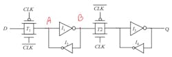
This is a common flip-flop circuit consisting of a master and a slave latch, each of them having back-to-back inverters. Under normal and correct operation, while the clock is low, the transmission gate T1 is open and the input signal D is being fed to the master’s I1 and I2 inverters’ closed loop.
On the rising edge of the clock, the T1 transmission gate closes and T2 opens. The rectified input signal in the master subsequently travels to the slave latch and is reflected at the output Q after a period equal to the flip-flop propagation time, TPCQ.
Now assume that the clock is low, and the input D and node A have a state of logic 1, while node B is having a state of logic 0. Once input D changes to logic 0, node A voltage will start to fall and node B will start to rise in return.
If input D’s transition happens close to the active edge of the clock, T1 will close before nodes A and B complete the transition to their logic state of 0 and 1. They might become metastable and stuck at an intermediate voltage value between 1 and 0, taking indefinite time to settle randomly to one of these two states.
Modeling the Metastability
To better understand metastability and how long the latch will take to stabilize and exit metastability, let’s model the inverters as negative amplifiers, with gain G driving resistance R and capacitive load C of the transmission gate and the other inverter (Fig. 2). For simplicity, assume the inverter’s PMOS and NMOS driving strength and threshold voltage are equal, having a middle point voltage Vm = VDD/2. Then solve for the voltage difference between node A and B.
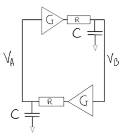
According to Reference 2, the system can be modeled by:
where ΔVin is the voltage difference between nodes A and B at the moment the active clock edge cuts off the D input from the node A, and ΔVout is the voltage difference between the two nodes after time t.
The time td takes for the voltage difference to reach VDD and resolve metastability, by having node A and B resolve to either 0 or 1, for a ΔVin input voltage difference, can be given by:
Figure 3 represents the relationship between the starting voltage difference and time.
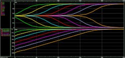
The starting voltage difference vs time is shown in Figure 3. For a relatively large ΔVin, nodes A and B are quickly resolved to 1 and 0, and for a very small ΔVin, it takes quite a while to resolve the metastability. Equation 1 states that the output voltage difference ΔVout depends on ΔVin.
The top picture in Figure 3 might appear a bit counterintuitive, but that’s because the exponential growth is on a very tiny scale. The bottom picture is more illustrative; it depicts the voltage difference between the nodes represented on a logarithmic scale.
>>Download the PDF of this article

Equation 2 also states that if the input voltage difference was 0, e.g., both nodes A and B had a voltage of 0.5, it would take forever, and we won’t be able to resolve the metastability. That shouldn’t be much of a concern, though. Even if the rising clock edge cuts off the input signal while both nodes are at 0.5 V, a slight thermal noise could offset any of these points, allowing the metastability to be resolved eventually.
To sum up, when data is being sent between two clock domains having different phase or frequency, the asynchronous signal might toggle during the capture clock transition. This leads the output to be metastable and oscillate in an intermediate value between 1 and 0 before settling down randomly, after time td given by Equation 2. It’s important for the metastability to settle to a legal value before passing through any combinational logic to avoid its propagation down the logic stream.
What’s the Probability of Entering the Metastable State?
With the understanding that metastability can’t be avoided, and knowing how long it will take us to exit this state, let’s look into the probability of entering the metastable state in the first place, as well as the probability of not being able to resolve it in the required time, leading to logic failure.
Say we have a clock period of TC and that any change in the data input during aperture time TA will cause metastability.3 The probability of entering metastability thus would be the time in which we could enter the metastable state divided by the total time, given by:
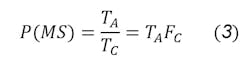
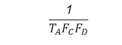
where FC is the clock frequency of the design. Since the input D won’t be changing every clock cycle, a changing rate of FD — the rate for entering metastability — per second, would be:

And the mean time between entering metastability would be:
For a design with a clock frequency of 2 GHz, with a flip-flop setup and hold time of 15 ps and 5 ps, respectively, the probability of entering metastability would be 0.04. For an input with a changing rate of 400 MHz (0.4 × 10⁹), the latch will be metastable 16 × 106/sec, meaning the design will enter metastability once every 125 clock cycles, which is quite often.
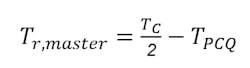
To calculate the probability to fail metastability, we need to define resolution time Tr, which is the time the master latch must resolve nodes A and B before metastability is propagated to the slave latch. Tr, master would be given by half the clock cycle minus the setup time of the slave latch. The setup time of the slave latch would also be the flip-flop propagation time TPCQ, which is the propagation delay through T2 and I3:
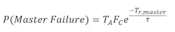
The probability of the master latch to fail to resolve the metastability would then be the probability of entering the metastability and the probability of not being able to resolve it in a time Tr.
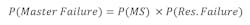
The probability of not being able to resolve the metastability can be derived the same way P(MS) was derived. Looking at Equation 1, assuming ΔVin,min is needed to resolve the metastability before time Tr and assuming all ΔVin possible values have equal probability, then the probability of failure of resolving the metastability before Tr would be:
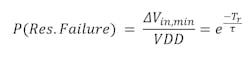
And the probability of failure would be given by:
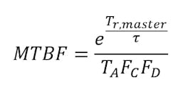
Also, the mean time between failures would be:
Now, to find the probability of failure of a flip-flop, that would involve the probability of the master latch to enter metastability and fail to resolve it, as well as the slave latch. The probability would be given by:
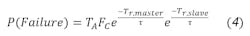
where Tr, slave is given by:
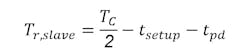
where tsetup is the setup time of the second flip-flop, and tpd is the stage delay from the slave latch, or the output of the first flip-flop, until the input of the second flip-flop. We can say that Tr, flop is the time needed by the flip-flop to resolve the metastability, given by:
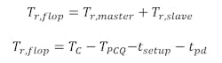
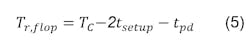
For identical flip-flops and master/slave latches, Tr, flop can be given by:
Now the probability of one-stage flip-flop synchronizer failure can be given by:
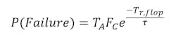
Assuming τ = 35 ps and tpd = 0, then Tr, flop = 500 – (2 * 15) = 470 ps. The probability of the synchronizer mentioned above to fail is 58.9 × 10⁻⁹ with a failure rate of 23.6/sec, and the mean time between failure given by:
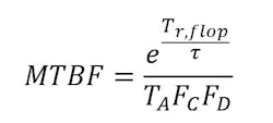
would be 42.4 ms, which is very low.
To sum up, when data is being transferred from one clock domain to another, the probability of entering metastability could be given by Equation 3, which will lead the output of the flip-flop to become unstable until time td, given by Equation 2.
Flip-Flop Synchronizers
If a one-stage flip-flop synchronizer takes time td more than one clock cycle and isn’t able to resolve the metastability by then, or its MTBF is small, more flip-flop stages can be added. This would increase the overall time (Tr, sync) the synchronizer has to resolve the metastability before its propagation down the logic stream. It ultimately decreases the probability of the overall failure and increases the MTBF.
For an n-stages synchronizer, the probability of failure would simply be the probability of the previous synchronizers failing to resolve the metastability, multiplied by the probability of the last synchronizer stage to fail — the same as Equation 4. Assuming identical flip-flops are used having the resolution time Tr, the exponential term would simply be multiplied by the additional number of stages. The probability of failure and MTBF would be given by:
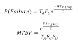
If we were to apply another synchronizer stage in the previous example, we would have an MTBF of 8 hours, and another stage will result in an MTBF of 621 years. Notice the exponential growth of the meantime between the synchronizer failure since the resolution time of the metastability increases in the exponential term e.
After calculating the previous MTBF and getting a value of around 600 years, it might seem that we’re on the safe side, and it would be a long time before metastability occurs and the system fails. However, unfortunately, that’s not the case.
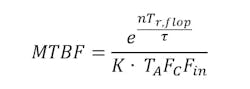
The total number of synchronizers in the design affects the overall MTBF. If we design a synchronizer with an MTBF of 600 years, but we have 600 synchronizers in the design, the actual MTBF of the design would be just one year, as we could have one synchronizer failing each year.
While designing the system and the architecture of the synchronizer, it’s important to consider how many synchronizers are going to be used and then calculate how that will affect the overall design’s MTBF to avoid any unforeseen failures. The MTBF for a design with K synchronizers would be given by:
Conclusion
Since metastability is unavoidable during clock domain crossing, mitigating its impact is vital for design reliability. Understanding the probability of your design to enter the metastable state and the probability of its failure is crucial in choosing or designing a synchronizer with high MTBF to ensure design reliability and robustness.
This article was supervised by Ahmed Abdelfattah, Senior Manager, Digital Implementation, Si-Vision.
References
1. Rabaey, J. M., Chandrakasan, A., & Nikolic, B. (2003), Digital Integrated Circuits: A Design Perspective.
2. Ginosar, R. (2011), “Metastability and Synchronizers: A Tutorial,” IEEE Design & Test of Computers, 28(5), 23–35, https://doi.org/10.1109/mdt.2011.113.
3. D. Harris and S. Harris, Digital Design and Computer Architecture: ARM Edition. Morgan Kaufmann, 2015.
>>Download the PDF of this article
About the Author
SeifEldeen Emad Abdalazeem
Senior ASIC Physical Design Engineer, Si-Vision
SeifEldeen Emad Abdalazeem holds a Bachelor's degree in Nanotechnology and Nanoelectronics Engineering from Zewail City of Science and Technology, Cairo, Egypt. He specializes in PnR, STA timing analysis, and design closure on advanced technology nodes and high-speed designs.
Comment About the Article
To join the conversation, and become an exclusive member of Electronic Design, create an account today!

Leaders relevant to this article: