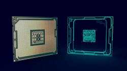
Can Digital Twins Recreate Everything Down to the Chip?
What you'll learn:
- The expanding role of digital twins in software-designed architectures.
- Siemens EDA's digital-twin strategy and the role of AI.
- How the company is opening the door to AI-powered multi-domain design engineering.
The rapid shift to software-defined architectures in cars, robots, and everything in between is changing how chips are designed and how systems are assembled around them. The shift is elevating the role of digital twins in engineering, said Craig Johnson, VP of EDA Strategy at Siemens EDA. He added that keeping up with the semiconductor industry’s explosive growth, projected to hit $2 trillion by 2035, could come down to how widely they’re adopted.
As electronic systems grow more complex, the challenge for engineers is to figure out the tradeoffs between different designs and the implications at the chip, package, board, and system levels — all while racing against tight deadlines.
While power, performance, and cost are the main tradeoffs, they must be balanced against other factors, such as thermal behavior. Engineers are also keen to zoom in and zoom out of different segments of a design to see where things are working and where they’re not.
Digital twins will be key to keeping up with the complexity, said Johnson. Most electronic design automation (EDA) companies are working on ways to create chip-level digital twins, integrate them into package-level models, and then connect them to the product level to simulate everything from power distribution to heat dissipation. Instead of recreating all system components in isolation, engineers can use these digital twins to evaluate system-wide tradeoffs earlier in the design process.
According to Johnson, the thermal, mechanical, and electrical characteristics of a system can no longer be viewed separately. For instance, the heat generated by a processor can stress the circuit board, raising the risk of warping. In turn, that can impact electrical performance, creating a closed loop that drives the temperatures in the system, which can cause the processor to overheat.
Understanding the interplays between all of these variables helps engineers get the most out of both the silicon and the larger system.
Editor-in-Chief Bill Wong met with Johnson about the company’s strategy for digital twins and where AI fits into them. Johnson also explained what he wants to do over the long term: Give engineers the ability to run software on digital twins to see how everything works and where improvements can be made. That way, more of the design can be done before building a physical prototype. Part of the goal is to close the speed gap between software and hardware development.
This interview has been edited for clarity.
What’s happening in today’s EDA industry with regard to semiconductor innovation?
We all know this, but it’s something you’re starting to hear more from outside the semiconductor industry: Modern technological products simply can't exist without chips. They are the keys unlocking everything from AI to electric vehicles, renewable energy, and next-generation aerospace and defense systems.
The demand for smaller, faster, more efficient chips — along with the push to integrate AI so that companies can develop products more rapidly — is stretching the limits of electronic design and manufacturing. That includes pressure on cost efficiency and sustainability goals.
At the same time, the broader industry is dealing with increasingly complex design requirements, constrained resources, tighter sustainability regulations, and ongoing supply-chain challenges, all of which put added strain on design cycles.
Our customers are trying to bring more predictability to their development timelines, compressing what used to take 18 to 36 months down to 12 to 18 months for both development and delivery. That’s why we’re striving to reduce semiconductor time-to-market with AI-powered software solutions, including EDA tools.
Software is becoming a key source of differentiation in areas like automotive. How does a software-defined approach apply to the semiconductor industry?
This is one of the biggest trends across industries. Systems integrators are seeking value by product differentiation through software. For instance, automakers are adding a lot of new features and functions into cars between advanced driver-assist systems, infotainment, and personalized driver and passenger experiences.
OEMs need to determine how to design and simulate these capabilities to ensure the best performance. While product personalization happens in software, the differentiation starts with hardware.
In this environment, the traditional approach of designing hardware first and then adapting the software to it is no longer feasible with the advancements in modern computing, AI, and other high-performance applications. Software-defined systems are transforming the landscape of electronics development with hardware now dependent on software architecture.
Software workloads drive hardware architecture decisions from the earliest stages of design, where virtual representations of the semiconductor require experimentation to understand the compute platform that best optimizes the software. Adopting a software-defined methodology enables engineering teams to configure the entire system with software, including scaling limitations, multi-domain design and optimization, and maintaining data links across different levels of IC and system integration.
This is an exciting opportunity for companies leveraging EDA software as a competitive advantage over established companies that must adapt to a faster pace while dealing with legacy operations. Digital transformation and shift-left engineering are essential in the competitive global economy.
To effectively manage design complexity and deliver advanced electronics systems, companies must adopt strategies that accurately capture and model the system’s requirements as well as methods that support software-hardware co-design.
As chip-level scaling faces constraints, the integration of chiplets and 3D IC design workflows is crucial. We are seeing a major shift in the semiconductor industry and addressing these challenges with robust software-defined, AI-powered, silicon-enabled solutions.
How is Siemens EDA enabling AI-powered multi-domain design engineering?
Developing next-generation chips is an expensive process. But it’s a necessary one because more electronic systems and products rely increasingly on software, and the software needs to sit somewhere.
The complexity at every step of the development process — from designing and manufacturing the chips to packaging and implementing them on a PCB — is increasing exponentially. As a result, companies need to embrace a multi-domain engineering approach.
What that means in practice is integrating software, mechanical, and electronic design to manage the growing complexities of what we started calling a “system of systems.” AI is integral to closing the semiconductor engineering gap by connecting systems capabilities for operations, networking, power management, security, monitoring, learning, verification, validation, and testing across domains.
Managing cross-domain data within the context of a silicon lifecycle necessitates integration with broader platforms, while also gaining domain-specific insights.
For example, it’s essential for design engineers to build scalability and flexibility into both software and hardware to enable product lifecycle management. With a more software-defined approach to engineering, teams can monitor and impact real-world operating conditions as the product is in full operation. Integrating active monitors in semiconductors allows manufacturers to track performance and reliability, ensuring that products operate as intended and maintain up-to-date functionally throughout their product lifecycle.
We have been deploying AI to varying degrees in computer-aided chip design and manufacturing for decades now — all to help our customers deliver better products globally.
How does a digital twin apply for semiconductor design and manufacturing?
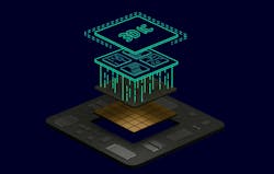
A digital twin is a physics-based digital representation of a process or a product; in short, a virtual copy of a physical or soon-to-be physical thing. While building a digital twin of any one part of a larger system is valuable — the processor at the heart of a car’s autonomous driving system, or the circuit board it sits on, or the vehicle as a whole — what we want is a comprehensive digital twin that encompasses all cross-domain models and data, from mechanical CAD and CAE to software code, bills-of-materials, bills-of-process, and more.
This approach creates a precise virtual representation matching the physical form, functions, and behavior of products and their configurations. Customers who adopt a comprehensive digital twin can reduce the need for physical prototypes during development by defining and optimizing the product in a virtual world, saving valuable time and resources.
Then, throughout the product’s lifecycle, updates to the digital twin reflect any changes to its physical counterpart, and vice versa, creating a closed feedback loop between the virtual and real environment. This opens the door to the continuous optimization of products and even production and supply-chain processes cost-effectively.
How will engineers and others involved in the product design actually use these digital twins? In practice?
With this seamless integration of products and production, including software and automation, manufacturers can design, simulate, test, and validate products using a comprehensive digital twin to optimize product and process quality while reducing design cycles. Semiconductor and systems companies can achieve more than just visual fidelity or simulation accuracy — it’s the unprecedented breadth and depth of integration across domains, processes, and lifecycles.
Where many EDA vendors offer fragmented capabilities limited to specific functions or processes, a comprehensive digital twin delivers a connected ecosystem spanning design through operation. Siemens’ comprehensive digital-twin enablement delivers a virtual representation of the product or process flow that matches the exact physical form, functions, and behavior of the product and its configurations while participating across the product and process lifecycle to simulate, predict, and optimize the product and production system.
Maybe most critically, it connects real-world operational data back into product design and production over the lifetime of the product, creating a self-improving system that most digital software vendors cannot provide.
The other part of the equation is what we call “digital threads,” which consolidate data across the lifecycle of a product from design to manufacturing and beyond. We can tie together this usually isolated data to improve the accuracy of the comprehensive digital twin.
By mirroring the physical world in the virtual world with digital threads, engineering teams can predict the performance and optimize the product in a proven and secure manner. Thus, automating tasks is achieved, and functions are interconnected, integrated, and linked so that engineering teams can quickly access, share, and manage their program details across the entire product lifecycle.
These digital threads provide a complete end-to-end process for a given industry. With digital twins stitched together by digital threads, companies will have a real-time digital backbone for optimizing design, manufacturing, testing, and maintenance of these complex systems. We are unique in bringing together PLM and EDA software as well as industry expertise and services that address specific complexity needs of the whole ecosystem, from semiconductor firms to electronics makers to their partners.
What other software technologies do you think will make a difference in the semiconductor market? What are you exploring going forward?
As electronics and semiconductor manufacturers deal with more complex market demands, ongoing supply-chain issues, and sustainability imperatives, how fully they implement digital twins is becoming a real differentiator. When data from across the organization is connected and accessible, decision-makers gain a lot more transparency and visibility, making it easier to integrate industrial-grade AI tools and potentially — although it’s a lot further out — move more engineering work into the metaverse.
The goal is to get AI to take on routine tasks, speed up product and process evaluations, and make it easier for people to learn new tools. This is particularly crucial with the aging and retiring workforce along with engineering talent shortages and skill gaps. And anticipated for the future of manufacturing, the metaverse is all about bringing together digital twins, AI, and software-defined automation to create an intuitive and collaborative virtual design and build environment.
Pressure across industries isn’t easing anytime soon. Recent geopolitical tariffs are likely to continue affecting global business, particularly for the electronics and semiconductor sectors. As companies try to tackle rising costs and more complex designs with limited engineering resources, they are likely going to need digital twins to keep up with innovation and time-to-market expectations. But that’s only going to be the first step of many in their digital transformation.
About the Author

William G. Wong
Senior Content Director - Electronic Design and Microwaves & RF
I am Editor of Electronic Design focusing on embedded, software, and systems. As Senior Content Director, I also manage Microwaves & RF and I work with a great team of editors to provide engineers, programmers, developers and technical managers with interesting and useful articles and videos on a regular basis. Check out our free newsletters to see the latest content.
You can send press releases for new products for possible coverage on the website. I am also interested in receiving contributed articles for publishing on our website. Use our template and send to me along with a signed release form.
Check out my blog, AltEmbedded on Electronic Design, as well as his latest articles on this site that are listed below.
You can visit my social media via these links:
- AltEmbedded on Electronic Design
- Bill Wong on Facebook
- @AltEmbedded on Twitter
- Bill Wong on LinkedIn
I earned a Bachelor of Electrical Engineering at the Georgia Institute of Technology and a Masters in Computer Science from Rutgers University. I still do a bit of programming using everything from C and C++ to Rust and Ada/SPARK. I do a bit of PHP programming for Drupal websites. I have posted a few Drupal modules.
I still get a hand on software and electronic hardware. Some of this can be found on our Kit Close-Up video series. You can also see me on many of our TechXchange Talk videos. I am interested in a range of projects from robotics to artificial intelligence.

Craig Johnson
VP, EDA Strategy, Siemens EDA
Craig Johnson joined Siemens in 2021 and is the VP of Strategy for Siemens EDA. He joined Cadence in 2004where he held leadership roles in strategic planning, marketing, M&A, and IT. Prior to Cadence, Craig worked in strategic marketing and operations at Intel. Craig holds MBA and B.S. degrees in electrical and computer engineering from Brigham Young University.

James Morra
Senior Editor
James Morra is the senior editor for Electronic Design, covering the semiconductor industry and new technology trends, with a focus on power electronics and power management. He also reports on the business behind electrical engineering, including the electronics supply chain. He joined Electronic Design in 2015 and is based in Chicago, Illinois.
Comment About the Article
To join the conversation, and become an exclusive member of Electronic Design, create an account today!

Leaders relevant to this article: