eGaN® FET-Silicon Power Shoot-Out Vol. 13, Part 1: Impact Of Parasitics
In a traditional hard switching transition, the switching losses are impacted by two device parameters, QGD, known as the Miller charge, which controls the voltage rising and falling speed; and QGS2, which is the portion of the gate to source charge from the device threshold voltage to the gate plateau voltage, which controls the current rising and falling speed. The turn off period, shown in Fig. 1a, begins with a decrease of gate drive voltage; when the gate to source voltage reaches the plateau, the voltage across the device will begin to rise, being driven by the gate current, IG.
Fig. 1. Ideal hard switching showing: (a) Turn-off transition and (b) Turn-on transition.
During the voltage rising period, the device encounters both current and voltage in the device, resulting in switching loss. For the voltage rising period, the device parameter determining loss is QGD. When the device voltage reaches the input voltage, the current in the device will begin to fall and more switching loss in the device will be incurred. For the current falling period, the device parameter determining loss is QGS2. The power loss during the turn off switching transition can be given by:
Where:
VIN =Input voltage (V)
IOFF = Turn-off current (A)
QGD = Miller charge (C)
QGS2 = Gate-to-source charge from device threshold voltage to gate
plateau voltage (C)
IG = Gate current (A)
For the turn on switching losses, the same principles apply, as shown in Fig. 1b. Minimizing the QGD and QGS2 parameters decrease switching losses incurred in a hard switching application. The turn on loss is given by:
Where:
ION = turn on current (A)
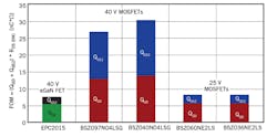
Figure of merit (FOM) is widely used to compare the performance of competing power devices[5]. The FOM of hard switching applications such as a synchronous buck converter is defined as the product of the dynamic loss parameters, QGD + QGS2, and static losses, RDS(ON). When comparing 40 V eGaN FETs to 40 V MOSFETs currently on the market, eGaN FETs offer a significant reduction in FOM, as shown in Fig. 2.
Fig. 2. 40 V device Figure of Merit comparison with VDS = 12 V, IDS = 20 A.
For designs requiring lower input voltages, for example a 12 V input buck converter, lower voltage MOSFETs can be utilized. The FOM of a 25 V Si MOSFET is comparable to a higher rated 40 V eGaN FET.
From an FOM comparison, the eGaN FET should achieve higher efficiency than the equally rated 40 V MOSFET devices and similar efficiency to the 40% lower rated 25 V MOSFETs. In practical applications, FOM is just one of the contributors to achieving higher efficiency. The others are die size optimization [6], package parasitics, and PCB layout parasitics. To enable the high switching speed available from low FOM, low parasitic packaging and PCB layout is required. eGaN FETs were developed in advanced land grid array (LGA) packages that not only have low internal inductance, but enable the user to design ultra-low inductance into their board. This shootout will cover the impact of package and PCB layout parasitics on converter performance and compare the in circuit performance of eGaN FET and MOSFET devices.
To evaluate the performance of the 40 V eGaN FET against different combinations of 40 V and 25 V MOSFETs, similar power loop designs were tested for the eGaN FET and MOSFETs. Fig. 3 shows the PCB layout for the designs with the high frequency loop highlighted in red in Fig. 3a.
Fig. 3.Conventional vertical power loop PCB layouts including: (a) side view showing high frequency loop in red, (b) MOSFET layout top view, and (c) eGaN FET layout top view.
This conventional PCB layout places the input capacitors and devices on opposite sides of the PCB, with the capacitors being located directly underneath the devices to minimize the physical loop size, leading to reduced PCB parasitic inductance. Space is left in between the devices for the switching node connection which is connected to the output inductor in a buck converter.
The eGaN FET and MOSFET prototypes, shown in Figs. 3b and 3c, used similar part layouts and identical board builds to ensure the comparison would only be influenced by the devices. For the MOSFET device, the smallest package was chosen, a 3 x 3 mm TSDSON-8, to compare against the eGaN FET 4.1 x 1.6 mm LGA package. For the drivers, the eGaN FET used the LM5113, designed to meet the driving requirements of the eGaN FET, while the MOSFET employed an ISL2111 MOSFET driver.
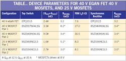
For the device comparisons, MOSFETs with similar on resistance were selected for the synchronous rectifiers and two different criteria were used to compare the top switch. The first criterion for the MOSFET top switch selection was to minimize dynamic loss parameters, QGD + QGS2, in an effort to offer the lowest switching losses at higher switching frequencies. The second criterion for MOSFET top switch selection was to select similar on resistance characteristics as the 40 V eGaN FET, to offer similar conduction losses. The selected devices and their characteristics are shown in the table.
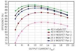
Fig. 4 compares the efficiency of the 40 V eGaN FET, 40 V MOSFETs, and 25 V MOSFETs, with the device parameters for these parts shown in the table.
Fig. 4. Comparing efficiency of 40 V eGaN FET and 40 V and 25 V silicon MOSFETs at VIN = 12 V, VOUT = 1.2 V, FSW = 1 MHz, LBUCK = 300 nH.
At a switching frequency of 1 MHz, the eGaN FET provided higher efficiency than all of the benchmark MOSFETs. The 40 V eGaN FET can outperform the best pair of 25 V MOSFETs by almost 1% and the best pair of 40 V MOSFETs by almost 3%. To explain the performance gains of the eGaN FET over the MOSFETs with similar FOM and a more optimized die size selection, the influence of package parasitics and PCB layout parasitics must be considered. For the eGaN FETs, switching losses can be reduced at higher frequencies by using the EPC2014 for the top switch, an eGaN FET with a smaller switching charge.
Converter Parasitics
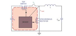
Previously, it was shown that devices with similar switching charges and on resistances performed differently in circuit. This can be seen by the greater than one percent difference in efficiency between the 40 V eGaN FET and the lower rated 25 V MOSFET pair 2. The reason for the improved performance of the eGaN FET when compared to a MOSFET with similar characteristics is the use of superior eGaN FET packaging. In a practical buck converter, there are two major parasitic inductances (see Fig. 5), which have a significant impact on converter performance:
Fig. 5.Synchronous buck converter showing parasitic inductances.
The first is common source inductance, LS, the inductance shared by the drain to source power current path and gate driver loop.
The second is high frequency power loop inductance, LLOOP, which is the power commutation loop and comprised of the parasitic inductance from the positive terminal of the input capacitance, through the top device, synchronous rectifier, ground loop, and input capacitor.
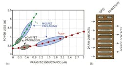
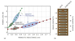
The common source inductance, Ls, has been shown to be critical to performance because it directly impacts the driving speed of the devices [7]-[9]. The common source inductance is mainly controlled by the package inductance of the device and varies from package to package [10], [11]. For the eGaN FET, the LGA package (Fig. 6b) offers low common source inductance, reducing loss, as shown in Fig. 6a.
Fig. 6. Parasitic Inductance vs Power Loss for eGaN and MOSFET packaging showing (a) Impact on power loss VIN = 12 V, VOUT = 1.2 V, IOUT = 20 A, FSW = 1 MHz, top switch EPC2015, synchronous rectifier EPC2015, and (b) the eGaN FET land grid array package.
The high frequency loop inductance, LLOOP, impacts the switching commutation time and the peak drain to source voltage spike of the devices. The high frequency loop inductance is controlled by the PCB layout and package inductance. In applications utilizing low package parasitics, e.g. eGaN FETs, the PCB layout dominates the high frequency loop inductance[12]-[15].
The impact of parasitic inductance on power loss for an eGaN FET based buck converter is calculated and shown in Fig. 6a [16], it can be seen that by introducing common source and high frequency loop inductance the loss increases. Understanding the impact of parasitic inductance on performance, the eGaN FET made the reduction of package parasitics a high priority. For the eGaN FET, a device with a higher voltage lateral structure, all of the connections are contained on the same side of the die. This allows for the die to be mounted directly to the PCB, minimizing the total parasitics to the internal bussing and external solder bumps. To further decrease parasitics, the drain and source connections are arranged in an interleaved LGA package, providing multiple parallel connections to the PCB from the die. The result is a device package inductance in the range of a couple hundred picohenries [5],[11].
PCB Layout
With the significant reduction in package related inductance provided by the eGaN FET, the common source inductance is minimized and is no longer the major contributor to parasitic loss. Instead, it is the high frequency loop inductance, controlled by PCB layout, thus making layout using the eGaN FETs critical to high frequency performance.
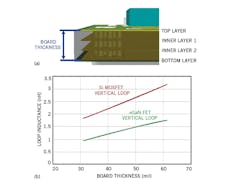
To compare the performance of different PCB layouts for both eGaN FETs and MOSFETs, two different board builds were considered based on the PCB layout in Fig. 3. For the layout comparison, a 4 layer PCB was used with two ounce copper on each layer and an overall board thickness of 62 and 31 mils were tested. In the conventional vertical power loop design, the loop inductance is heavily dependent on the board thickness as the power loop is contained on the top and bottom layers of the PCB. As the board thickness increases so does the high frequency loop inductance, leading to higher losses and consequently lower efficiency.
Fig. 7. Vertical power loop design: (a) PCB cross section and (b) simulated high frequency loop inductance vs board thickness.
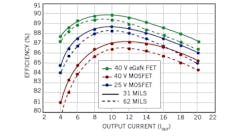
Fig. 7a shows the cross section of a circuit board, while Fig. 7 b shows the simulated high frequency loop induc tance of the eGaN FET and MOSFET based PCB designs. Due to the eGaN FET’s smaller size and reduced package parasitics, the loop inductance is reduced around 50% when compared to the MOSFET design. For the eGaN FET, the PCB layout dominates the loop inductance, with the inductance increasing 80% when the board thickness increases from 31 to 62 mils. As a result, the 62 mil board designs all suffer an efficiency drop of at least 1% (Fig. 8).
Fig. 8.Comparing efficiency vs output current for 40 V eGaN FET, 40 V MOSFET, and 25 V MOSFETS with VIN = 12 V, VOUT = 1.2 V, FSW = 1 MHz, and LBUCK = 300 nH.
While figure of merit is an important metric in determining the best performing device, the package and layout parasitics are also a major contributor to loss. In this article, eGaN FETs and MOSFETs were compared using similar traditional PCB layouts. The eGaN FET, combining low FOM, low package parasitics, and a small footprint reducing PCB parasitics, outperformed MOSFETs rated for much lower voltages. As FOM and packages improve, the PCB layout becomes critical to high efficiency.
The next part of this series on eGaN FETs explores the topic of PCB layout optimization to further improve the performance achievable with these high-performance eGaN FETs.
References
[1] J. Strydom, “The eGaN® FET-Silicon Power Shoot-Out Vol. 7: Buck Converters”, Power Electronics Technology, Vol. 38, No. 2, February, 2012.
[2]J. Strydom, “The eGaN® FET-Silicon Power Shoot-Out Vol. 8: Envelope Tracking Power Electronics Technology, Vol. 38, No. 5, May, 2012.
[3] M. de Rooij and J. Strydom, “eGaN® FET – Silicon Shoot-out Vol. 9: Wireless Power Converters,” Power Electronics Technology, Vol. 38, No. 7, July 2012.
[4] D. Reusch and J. Strydom, “The eGaN® FET-Silicon Power Shoot-Out Vol. 10: High Frequency Resonant Converters,” Power Electronics Technology, Vol. 38, No. 9, September 2012.
[5] J. Strydom, “The eGaN® FET-Silicon Power Shoot-Out Vol. 1: Comparing Figure of Merit (FOM),” Power Electronics Technology, Vol. 36, No 9, September 2010.
6] J. Strydom, “The eGaN® FET-Silicon Power Shoot-Out Vol. 11: Optimizing FET On-Resistance,” Power Electronics Technology, Vol. 38, No. 10, October 2012.
[7] A. Elbanhawy, “Effects of parasitic inductances on switching performance,” in Proc. PCIM Eur., May 2003, pp. 251–255.
[8] G. Nobauer, D. Ahlers, J. Sevillano-Ruiz, “A method to determine parasitic inductances in buck converter topologies,” in Proc. PCIM Eur., May 2004, pp. 37–41.
[9] B. Yang, J. Zhang, “Effect and utilization of common source inductance in synchronous rectification,” in Proc. IEEE APEC’05, Mar. 2005, vol. 3, pp. 1407–1411.
[10]M. Pavier, A. Woodworth, A. Sawle, R. Monteiro, C. Blake, and J. Chiu, “Understanding the effect of power MOSFET package parasitic on VRM circuit efficiency at frequencies above 1 MHz,” in Proc. PCIM Eur., May 2003, pp. 279–284.
[11]D. Reusch, D. Gilham, Y. Su and F.C. Lee, “Gallium nitride based multi-megahertz high density 3D point of load module,” APEC 2012.
pp. 38-45. Feb. 2012.
[12] T. Hashimoto, T. Kawashima, T. Uno, Y. Satou, N. Matsuura, “System in package with mounted capacitor for reduced parasitic inductance in voltage regulators,” Applied Power Electronics Conference and Exposition, 2008. APEC 2008. Twenty-Third Annual IEEE, pp.187-191, 24-28, Feb. 2008.
[13] Y. Kawaguchi, T. Kawano, H. Takei, S. Ono, A. Nakagawa, “Multi Chip Module with Minimum Parasitic Inductance for New Generation Voltage Regulator,” Power Semiconductor Devices and ICs, 2005.
[14] A. Ball, M. Lim, D. Gilham, F.C Lee, “System design of a 3D integrated non-isolated Point Of Load converter,” Applied Power Electronics Conference and Exposition, 2008. Twenty-Third Annual IEEE, pp.181-186, 24-28 Feb. 2008.
[15] D. Reusch, F.C. Lee, Y. Su, D. Gilham, “Optimization of a High Density Gallium Nitride Based Non-Isolated Point of Load Module,” Energy Conversion Congress and Exposition (ECCE), IEEE, Sept. 2012.
[16] D. Reusch, “High Frequency, High Power Density Integrated Point of Load and Bus Converters,” PhD Dissertation, Virginia Tech, 2012.
About the Author
Voice Your Opinion!
To join the conversation, and become an exclusive member of Electronic Design, create an account today!

Leaders relevant to this article:
