GaN Delivers More Compact Power Supplies
Check out Electronic Design's coverage of CES 2024. This article is also part of the TechXchange: Gallium Nitride (GaN).
What you’ll learn:
- Why Navitas Semiconductor’s GaN solution is unique.
- Why GaN-based power supplies are smaller and more efficient.
Gallium-nitride (GaN) transistors are able to handle large currents at high switching speeds, leading to switching power supplies that are significantly smaller than their silicon-based counterparts. That’s because faster switching speeds and lower on-resistance of GaN FET transistors let designers employ smaller magnetics, reducing the size of the solutions. Unfortunately, GaN transistors can be a bit fragile, requiring additional protection to provide a more robust solution.
I talked with Stephen Oliver, VP Corporate Marketing & Investor Relations at Navitas Semiconductor, about where the company’s latest GaN technology is being deployed (see video above).
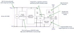
Improper use of GaN transistors can result in breakdowns, which has made GaN adoption more challenging to engineers. To address this situation, Navitas uses a system-in-package (SiP) approach that adds controlling electronics for the GaN transistor, which is also in the package (Fig. 1). This provides protection from electrostatic discharge (ESD) and other features, making it easier for designers to include it in their solutions.
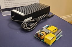
Such GaN-based solutions can be considerably smaller (Fig. 2) because they operate at a higher frequency than switching power supplies based on silicon transistors. The higher frequency means that the same power conversion can be done using smaller components like transformers and inductors. The SiP also provides lossless current-sensing support. Typically, this is done using a sensor based around a low-resistance resistor that consumes power, reducing the overall efficiency of the power supply.
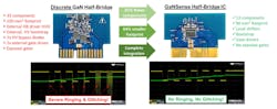
The same SiP approach is used in Navitas’s latest half-bridge solution, which provides the front end to a pair of integrated GaN FET transistors (Fig. 3). The low-profile, low-inductance SiP comes in a standard 6- × 8-mm PQFN package.

Among the features in its single-transistor solution are overcurrent protection and overtemperature protection (Fig. 4). The half-bridge can operate at megahertz speeds instead of the kilohertz switching speeds of silicon-based solutions.
Check out more of Electronic Design's coverage of CES 2024, and more videos/articles in the TechXchange: Gallium Nitride (GaN).
About the Author

William G. Wong
Senior Content Director - Electronic Design and Microwaves & RF
I am Editor of Electronic Design focusing on embedded, software, and systems. As Senior Content Director, I also manage Microwaves & RF and I work with a great team of editors to provide engineers, programmers, developers and technical managers with interesting and useful articles and videos on a regular basis. Check out our free newsletters to see the latest content.
You can send press releases for new products for possible coverage on the website. I am also interested in receiving contributed articles for publishing on our website. Use our template and send to me along with a signed release form.
Check out my blog, AltEmbedded on Electronic Design, as well as his latest articles on this site that are listed below.
You can visit my social media via these links:
- AltEmbedded on Electronic Design
- Bill Wong on Facebook
- @AltEmbedded on Twitter
- Bill Wong on LinkedIn
I earned a Bachelor of Electrical Engineering at the Georgia Institute of Technology and a Masters in Computer Science from Rutgers University. I still do a bit of programming using everything from C and C++ to Rust and Ada/SPARK. I do a bit of PHP programming for Drupal websites. I have posted a few Drupal modules.
I still get a hand on software and electronic hardware. Some of this can be found on our Kit Close-Up video series. You can also see me on many of our TechXchange Talk videos. I am interested in a range of projects from robotics to artificial intelligence.