New Thermal-design Options Drive Power Density

Across virtually all electronic product segments, system designers compete to deliver ever-greater functional densities.To keep the power subsystem from subsuming an increasingly large fraction of the product package, power densities must increase at an even greater rate than do functional densities. This trend, unfortunately, exacerbates the challenging thermal-design task product development teams already face.
The heat that power components generate is potentially problematic on several levels of the design hierarchy: Underperforming thermal designs result in high operating temperatures, which can reduce the reliability of power components and, in dense applications, other nearby devices. In environments characterized by elevated ambient temperatures, power derating reduces a power component’s realizable power capability, which at the system level, can manifest as larger, heavier, and more expensive systems. Thermal designs that are inefficient near the thermal points of origin can prompt compensations elsewhere in the system, such as increases in airflow requirements to maintain dissipative devices within their safe operating-temperature range. Increasing a cooling system’s airflow requirement also increases its energy use, increasing the system’s operating costs.
Related Articles
- Metal in the Board: Meeting the Challenge of Digital Power
- Proactive Thermal Management: The Right Time Is During Design
- Thermal Dissipation for DC-DC Conversion in Portable Designs
- How Hot is Too Hot? Ask Sherlock
The first line of defense, then, is to minimize heat generation throughout the power subsystem design. Highly efficient systems minimize I2R losses, starting at the power entry point. For example, 400 VDC power distribution in data centers and 270 VDC distribution in airborne systems reduce copper losses in power feeds below those of lower-voltage distribution systems. Efficient power-subsystem designs minimize the number of conversion stages from entry to load. They also take advantage of highly efficient power-conversion topologies such as ZVS (zero-voltage switching) and ZCS (zero-current switching).
Minimizing the number of conversion stages while accommodating high power-entry voltages and maintaining high conversion efficiency can challenge traditional converter designs. Fortunately, these high voltage-ratio applications have given rise to alternative power architectures and conversion topologies.
For example, a SAC™ (Sine Amplitude Converter™) can provide high voltage ratio conversion while delivering higher efficiency and lower output ripple than traditional topologies (Fig. 1).
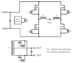
For example, Vicor’s VTM implementation of the SAC topology can provide fixed voltage ratios between 1:1 and 40:1 allowing direct 48 to 1.2 V conversion for POL applications at up to 98% efficiency.
This approach reduces output ripple by about 1/3, substantially reduces the noise energy at harmonics of the switching frequency, and provides about five times faster load-step response than traditional topologies. Such performance greatly reduces the need for output bulk capacitance, which reduces the system cost. It also allows for a tighter circuit-board layout, which helps reduce I2R losses in the highest current section of the power subsystem—the point of load. Overall, taking advantage of such technologies can reduce heat-generating conversion losses by as much as 40% compared to traditional power-conversion schemes.
Keep Cool
In the end, no matter how efficiently your power subsystem delivers energy from entry to load, the residual dissipation, the heat it generates, and your ability to remove that heat from the system limits your design’s power density. Once generated, there are two basic methods of removing heat from the power subsystem: convection and conduction.
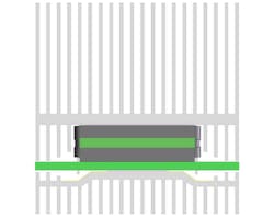
The effectiveness of convection cooling—blowing air across the device’s top surface—is dependent on inlet air temperature, airflow rate, airflow impedances or disruptions, and the device’s case temperature. Conduction cooling hinges on a thermo-mechanical connection to draw heat from a higher temperature locale to a cooler one. Its effectiveness is dependent on heat sink size and material, the thermal interface material and thickness, the device temperature, and the external temperature (Fig. 2).
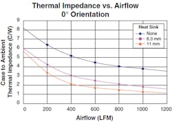
For devices that use heat sinks that are wholly contained within the system chassis, cooling is ultimately a two-stage process: conduction from device to heat sink and convection from heat sink to ambient. Thermal calculations must take both stages into account, an issue that some power-converter manufacturers mitigate by providing heat sinks or references to commercial suppliers’ catalog parts.
Design-support tools can range from simple tables and charts to sophisticated simulation software. Manufacturer’s thermal-performance graphs can provide quick and useful insight into a power component’s performance under a variety of configurations and operating conditions. Derating curves for no-heat-sink operation (Fig. 3a) and for operation with manufacturer-specified heat sinks (Fig. 3b)
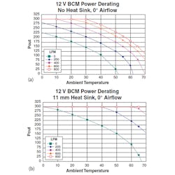
allow you to align your thermal and electrical designs. They help coordinate these two aspects of your product’s performance at the very start of the design cycle and give the electrical- and thermo-mechanical-design members of your team important data with which to balance design tradeoffs.
General-purpose tools, such as FEA (finite-elements array) analyzers, can model and simulate virtually any configuration and thermal design. But FEA tools tend to be expensive and require specialized knowledge to use effectively. Product-centric analysis tools, by contrast, are often free of charge and take mere minutes to learn.
The tradeoff is that these tools are usually specific to a particular manufacturer’s product lines and may limit the thermo-mechanical configurations you can simulate. This restriction, however, has a silver lining: By limiting the thermo-mechanical design, the manufacturer-supplied simulation tools can guide you to those that the manufacturer has developed and proven effective, potentially saving you a substantial fraction of the thermal-design schedule and engineering costs.
One example of such simulation tools is Vicor’s PowerBench™ simulator, which provides seven simulation types: VIN startup, EN (enable) startup, EN shutdown, VIN step, load step, steady state, and thermal. The Power Bench simulation environment provides an application circuit with user settable operating conditions for source and load and adjustable parameters for input- and output-circuit components (Fig. 4).
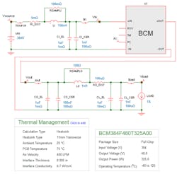
The thermal simulation shown provides means to select between designs using a 6.3-mm or 11-mm heat sink or a cold plate. You can also set the ambient temperature, circuit board temperature, air velocity, interface thickness, and interface conductivity. Among the output data the thermal simulation provides are the output power, power loss, efficiency, heat loss through the case, heat loss through the circuit board, and device operating temperature.
The simulation results from Fig. 4 report that the circuit delivers 326 W to its load with an efficiency of 95.54%, resulting in 15.21 W of power loss. The simulation calculates the power component’s operating temperature under the stated conditions at 80 °C—only 5 °C warmer than the circuit board, indicative of the power converter’s high efficiency and the heat sink’s efficacy.
Power Packaging
Most components, and certainly most power-dissipating components, within power conversion modules mount to the top side of the converter’s printed-circuit board. For simplicity of design, most product designs cool power modules and power ICs through their top surfaces.
There are, however, multiple paths available for sinking heat out of and away from power converters. As a product’s requirements push power densities higher, thermal designs more sophisticated than simple topside cooling take advantage of other options.
In many power converter structures, the majority of dissipated energy is attributable to power MOSFETs and power-carrying electromagnetic components. Fortunately, these parts usually connect directly to the pins that form the device’s electrical and mechanical interfaces to the circuit board. The same pins can conduct heat out of a power converter’s package if the underlying circuit board design provides appropriate thermal features.
For heat conduction through the power package’s pins, through-hole mounting is more efficient than surface mount but both technologies can provide useful contributions to the product’s thermal performance. The circuit board’s design must account for the additional heat from the power devices and the proximity of those devices to other dissipative components, such as processors.
New power packaging technologies and their associated materials allow for an important departure from topside dominant cooling. Power-train designs that arrange dissipative components symmetrically on both sides of a module’s circuit board coupled with highly thermally conductive packaging materials allow substantial cooling through the package’s top and bottom surfaces. An additional benefit is that this arrangement can also shrink the layout within the module, increasing power density while simultaneously increasing efficiency by reducing I2R losses due to finite conductivity in the interconnecting copper traces.
One example of packaging currently available for two-sided cooling is Vicor’s new ChiP (Converter housed in Package) technology, which provides substantially the same thermal resistances through top and bottom surfaces (Fig. 5).

ChiP packaging supports a wide range of power-management functions including AC-DC conversion with PFC (power-factor correction); isolated bus conversion; DC-DC conversion; buck, boost, and buck-boost regulation; and PoL current multiplication (Fig. 6).

For power components that are thermally, not electrically, power limited, two-sided cooling can extend the device’s derating curve tens of degrees toward higher ambient operating temperatures. Conversely, for applications that can maintain modest ambient temperatures, two-sided cooling allows designers to exploit power components for extremely high power densities. The packaging technology is scalable with sizes ranging from 0623 (6 x 23 mm) to 6123 (61 x 23 mm) and expanding, output currents to 180 A, voltages to 430 V and rising, and power delivery to 1.5 kW and rising. With these characteristics, ChiP power components realize power densities up to 3 kW/in3 and area densities up to 850 W/in2 with efficiencies as high as 98%.
Power components exploiting ChiP technology can provide exceptional thermal performance in two-sided cooling applications (Fig. 7).
The thermal-management cell, depicted schematically in the figure, targets an RθJ-A (junction-to-ambient thermal resistance) less than 0.66 °C/W, allowing for dissipation greater than 60 W at 70 °C ambient. The thermal-management cell concept supports power densities in excess of 200 W/in3 and outputs to 1.8 kW/cell with 400 VDC inputs under the same ambient conditions. The cell uses a single 40- x 40-mm fan to cool both top and bottom heat sinks and is inherently scalable for larger outputs.
Recommendations
· Avoid heat generation where possible. High distribution voltages, highly efficient power components, minimum conversion stages, compact designs, and careful layout all help minimize power loss.
· Include thermo-mechanical design issues as early in your design cycle as possible. High power density is attainable if you make it a design priority at the beginning of the process.
· Choosing among multiple cooling options requires thermo-mechanical tradeoffs. Take your mechanical engineer to lunch.
· Take advantage of advanced power packaging technologies to realize the maximum benefits of two-sided cooling.
References:
1. Salato, Maurizio, The Sine Amplitude Converter™ Topology Provides Superior Efficiency and Power Density in Intermediate Bus Architecture Applications, Vicor Corporation, June 2011. http://cdn.vicorpower.com/documents/whitepapers/wp_sac.pdf
2. Oliver, Stephen, 3D Cooling of New High Density DC-DC Converters, APEC 2013 Conference, Long Beach CA, March 2013.
About the Author
Gary Gill
Vice President Marketing, BG Networks
Gary Gill is Vice President Marketing at BG Networks. Gary has held a broad range of roles from engineering to marketing and sales in both technology startups as well as established market leaders. His semiconductor marketing and sales experience includes roles at Analog Devices, NXP Semiconductors, and Vicor Corp.
Gary holds BS and MEng degrees in electrical engineering and computer science from the Massachusetts Institute of Technology as well as an MBA from Duke University.
Comment About the Article
To join the conversation, and become an exclusive member of Electronic Design, create an account today!

Leaders relevant to this article: