Nvidia’s GeForce 256: The First Fully Integrated GPU
This article is part of the Electronics History series: The Graphics Chip Chronicles.
The term "GPU" has been in use since at least the 1980s. Nvidia popularized it in 1999 by marketing the GeForce 256 add-in board (AIB) as the world’s first fully integrated graphics processing unit. It offered integrated transform, lighting, triangle setup/clipping, and rendering engines in a single-chip processor.
Very-large-scale integrated circuits, or VLSI, started taking hold of the semiconductor industry in the early 1990s. As the number of transistors engineers could cram on a single chip increased almost exponentially, the number of functions in the CPU and the graphics processor increased.
One of the biggest strains on the CPU was graphics transformation compute elements into graphics processors. Architects from various graphics chip companies decided transform-and-lighting (T&L) was a function that should be in the graphics processor. The operation was known at the time as transform and lighting (T&L). A T&L engine is a vertex shader and a geometry translator.
In 1997, 3Dlabs developed its Glint Gamma processor, the first programmable transform and lighting engine as part of its Glint workstation graphics chips, and it introduced the term GPU—geometry processor unit. The GPU was a separate chip named Delta (also known as the DMX). 3Dlabs’ GMX was a co-processor to the Glint rasterizer.
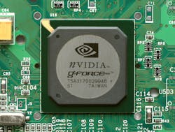
Then, in October 1999, Nvidia introduced the NV10 GPU with an integrated T&L engine for a new consumer graphics card. ATI quickly followed with their Radeon graphics chip and called it a visual processing unit—VPU. But Nvidia came out ahead in the terminology wars and has since been associated with the GPU and credited with inventing it.
Based on TSMC’s 220-nm process, the 120 MHz NV10 had 17 million transistors in a 139 mm² die and used DirectX 7.0. The GeForce 256 AIB employed the NV10 with SDR memory.
Before Nvidia started offering Nvidia-branded AIBs, the company depended on partners to build and sell the boards. However, Nvidia offered reference designs to its OEM partners.
The first AIB to use the 64 MB SDR was ELSA’s ERAZOR X which used its own design to create a NLX form factor board.
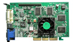
The GPU had a large 128-bit memory interface, and it could use DDR or SGRAM memory, a choice made by OEM board partners and usually done as a price-performance trade-off. The AIB shown in the above image has four 8 MB SGRAM chips. Since it was a 1999 AIB, it used the AGP 4X interface with sustained DMA, and supported the Direct3D 7.0 API and OpenGL 1.2.1 with transform & lighting.
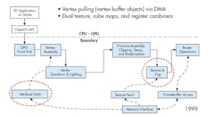
The chip had many advanced features, including four independent pipelined engines that ran at 120 MHz. That allowed the GPU to produce a 480 Mpix/sec fill rate. The video output was VGA. The chip also came with hardware alpha-blending and was HDTV compliant.
In addition to advanced graphical features, the chip also had a powerful video processing capability. It had a TV out capability and integrated NTSC/PAL encoders. It supported S-VHS and Composite video-input, and stereo 3D.
Integrating transform and lighting capability into the GPU was a significant differentiator for the GeForce 256. Before the stand-alone T&L processor from 3Dlabs, previous 3D accelerators used the CPU to run these functions. Incorporating the T&L capability reduced costs for consumer AIBs while at the same time improving performance.
Prior to the GF256, only professional AIBs designed for CAD had a T&L co-processor engine. It also expanded Nvidia’s market by allowing the company to professional graphics market. Nvidia marketed those AIBs as Quadro. The Quadro AIB used the same NV10 as the GeForce AIBs and used certified drivers for various professional graphics applications.
This article is part of the Electronics History series: The Graphics Chip Chronicles.
About the Author

Jon Peddie
President
Dr. Jon Peddie heads up Tiburon, Calif.-based Jon Peddie Research. Peddie lectures at numerous conferences on topics pertaining to graphics technology and the emerging trends in digital media technology. He is the former president of Siggraph Pioneers, and is also the author of several books. Peddie was recently honored by the CAD Society with a lifetime achievement award. Peddie is a senior and lifetime member of IEEE (joined in 1963), and a former chair of the IEEE Super Computer Committee. Contact him at [email protected].
Comment About the Article
To join the conversation, and become an exclusive member of Electronic Design, create an account today!

Leaders relevant to this article: