Memory Chip Makers Take 3D NAND Up a Level
Check out more coverage of the 2022 Flash Memory Summit.
Memory chip giants are upping the ante on each other with new generations of 3D NAND flash.
3D NAND chips resemble skyscrapers in which floors of flash-memory cells are stacked on top of each other. Memory chip manufacturers are stacking the chips even higher to cope with a world awash in data.
Ahead of the Flash Memory Summit, Micron said it entered mass production with its most advanced triple-level-cell (TLC) 3D NAND flash with 232 layers, translating to a 1 TB maximum per die.
The U.S. memory chip leader said the devices support about 40% more density than its 176-layer 3D NAND, which promises to pay dividends in everything from smartphones to data centers and the intelligent edge.
While the future of flash memory requires advances in memory controllers used to read, write, and erase data to storage drives and firmware to run on top of them, innovations in memory are at the heart of it all.
"The advancement of 3D NAND technology is crucial for innovation in the memory market,” said Gregory Wong, principal analyst at Forward Insights.
The world’s No. 3 memory chip maker, Micron currently leads when it comes to mass production of 3D NAND with more than 200 layers. But the competition sits close behind.
The Fourth Dimension
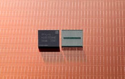
SK Hynix is boasting a new industry benchmark with a new generation of its "4D NAND" composed of 238 layers of NAND flash-memory cells. This is an upgrade from its 176-layer NAND released in 2020.

The world's second-largest memory chip maker is shipping samples of a 512-GB chip based on 238-layer TLC NAND to OEMs, with plans to start full production in the first half of 2023, slightly behind Micron.
The company claims its new offering is the "world’s highest layer-count NAND" and offers a smaller cell area per unit than other 3D NAND offerings. The improved density means higher bandwidth and power efficiency: The chips deliver a 50% improvement in data-transfer speed to 2.4 GB/s over previous-generation chips and power efficiency, too, as it cuts the amount of energy consumed while reading data in storage by 20%.
The chips will be used in client SSDs for PCs before being supplied for smartphones and high-end server SSDs. It plans to roll out with chips 1 TB of capacity next year, matching the capacity of Micron’s 3D NAND.
The new flash storage chip is referred to as a 4D NAND device by SK Hynix, because it is a 3D NAND design that places the peripheral CMOS logic that coordinates all the reading and writing operations underneath the memory cells, which are stacked on top of it. This is the company’s parlance for what Micron calls “CMOS-under-array” (CuA) technology, which allows more chips with higher density to be sliced from each wafer.
The memory cells are based on SK Hynix‘s “charge-trap flash” technology. In contrast to floating gate (FG), which stores electric charges in conductors, the technology stores electrical charges in tiny insulators to prevent interference between cells, improving read and write performance while giving a boost to density. For its part, Micron also uses the charge-trap flash format for its replacement-gate (RG) technology.
3D Packaged 3D NAND
Micron and other industry giants are also facing pressure from relatively new players in the flash market.
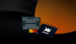
YMTC, backed by the Chinese state-conglomerate Tsinghua Unigroup, introduced the first in a new generation of NAND chips called X3-9070 that could help it compete with Micron, Samsung, and SK Hynix.
The new chip is based on its Xtacking 3.0 architecture, a heterogeneous 3D packaging technology that places the 3D NAND flash underneath a peripheral logic die that’s manufactured on a separate wafer and bonded to it with billions of tiny connections called vias. Xtacking 3.0 results in faster I/O while maximizing the density of its NAND, YMTC. On top of reducing die area, it helps improve latency and power efficiency.
China’s memory chip champion is currently shipping 64- and 128-layer products, presumably based on Xtacking 1.0 and 2.0. But this is its first to feature 232 layers, according to a report by government-backed Global Times.
YMTC declined to confirm many specifics about Xtacking 3.0, including the number of layers it supports.
According to YMTC, the new Xtacking 3.0 results in a 50% performance boost, topping out at 2,400 MT/s compared to its prior generation’s maximum of 1,600 MT/s, rivaling Micron’s and SK Hynix’s latest chips.
YMTC said the architecture also doubles storage density to 1 TB per chip that will pay dividends for SATA, PCIe SSDs, and eMMC and UFS for mobile and embedded flash. This is paired with a 25% drop in power consumption.
The company pins both the performance and power efficiency gains on its use of a 6-plane architecture instead of the more traditional 4-plane of the previous-generation chips.
A plane is a region inside a flash-memory chip that can respond to I/O requests independently. YMTC said the 6-plane architecture of the X3 will help improve the speed of both random-access and sequential I/O.
The X3-9070 opens the door for YMTC to supply its growing customer base in data centers, mobile devices, PCs, and other areas with more advanced NAND flash. The company said XStacking 3.0 also gives a boost to endurance, quality, and reliability to meet stringent testing standards, such as JEDEC.
Founded in 2017, YMTC is a relative upstart in the semiconductor industry with a NAND market share that remains in the single digits. But it could potentially disrupt the status quo in the world of flash memory, and it is aggressively expanding its production capacity to do so.
Moreover, YMTC has raised eyebrows for its very fast advances in research and development (R&D). Apple is reportedly considering it as a memory chip supplier, which would be a major boon for the company.
The chips also come as the U.S. turns up the pressure on China’s technology industry. The U.S. is reportedly weighing whether to forbid shipments of fab equipment that allow companies to build NAND chips with over 128 layers.
Banning shipments of such critical chip-making tools to China could deal a huge blow to YMTC’s ambitions. It may also hamper its efforts to expand production of 3D NAND flash based on Xtacking 3.0.
Storage-Class NAND Flash
Kioxia, which introduced the first NAND flash memory chip more than 30 years ago, is innovating around its BiCS Flash memory to help bridge the gap between high-capacity NAND and high-speed DRAM.
At the Flash Memory Summit, it rolled out the second generation of its “storage-class memory” (SCM) XL-FLASH technology, with plans to start mass production of chips with a maximum 256-GB capacity by 2023.
XL-FLASH falls into the category of persistent memory because it promises to close the gap between NAND and DRAM. While DRAM supports high-speed data rates and reduced latency, that performance comes at a high cost and at the expense of both power and memory capacity. XL-FLASH aims to address these issues.
Intel was also trying to blur the boundaries between DRAM and NAND with its Optane family of 3D XPoint chips, which it discontinued last month due to lagging demand for the technology co-devised with Micron.
Based on its BiCS FLASH 3D flash memory, Toshiba said that it has upgraded the new XL-FLASH with multi-level-cell (MLC) technology that can save two bits per cell, helping drive down the cost of the storage-class memory. It also increased the maximum number of planes that can operate independently compared to its previous generation. That allows for faster throughput when it comes to storing or fetching data from flash.
XL-FLASH will first be deployed in SSDs. It could also expand to memory-channel-attached devices that sit on the DRAM bus, such as future industry-standard non-volatile dual in-line memory modules (NVDIMMs).
In the future, it could also be possible to upgrade the XL-FLASH with the Compute Express Link (CXL) bus for the purposes of memory expansion. Up to eight layers can be stacked in a single package to boost capacity.
Check out more coverage of the 2022 Flash Memory Summit.
About the Author

James Morra
Senior Editor
James Morra is the senior editor for Electronic Design, covering the semiconductor industry and new technology trends, with a focus on power electronics and power management. He also reports on the business behind electrical engineering, including the electronics supply chain. He joined Electronic Design in 2015 and is based in Chicago, Illinois.
Comment About the Article
To join the conversation, and become an exclusive member of Electronic Design, create an account today!

Leaders relevant to this article: