Manage ASIC, SoC Design Risk with Leading-Edge Verification Services
This article is part of the TechXchange: Addressing Chip Verification Challenges
What you’ll learn:
- Value in design prototyping using FPGAs.
- Validating the design with firmware.
- How the process works.
- Identifying companies with the right experience and expertise in FPGA and design prototyping capabilities can help prevent costly respins.
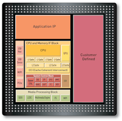
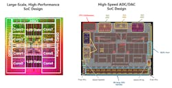
The performance benefits of advanced ASICs and SoCs (Fig. 1) are well-known to both the companies that develop them and their customers. So, the design challenges and risks that accompany a complex product design—bugs, flaws, and failure that can require costly respins—are worth assuming.
Managing those risks is critical in reducing or eliminating product delays and associated costs. One task all along the design timeline where risk can be reduced is prototyping and verification.
FPGA’s Value in Prototyping
FPGAs are useful for prototyping ASICs and SoC processors, and they’re proven to reduce the chance of delays and accelerate product time-to-market when used before and after a tapeout. The components required to work with a system-on-chip (SoC) are connected and tested with an FPGA prototype on a hardware platform. The chip design and firmware are reprogrammed until the SoC design is final and bug-free before the manufacturing of a final SoC begins.
Performance challenges found in the SoC’s connected components on the FPGA hardware platform are addressed by altering component selection, performance testing, and other actions so that performance can be verified before the chip returns from the foundry.
Chip verification is an essential part of the design cycle and needs to work in parallel. Verification can ensure that all parts or functionalities of the chip are working correctly.
Conventional verification techniques like RTL (register transfer level) simulations, gate-level simulations, system-level simulation, BIST (built-in self-test), DFT (design for testability) verification, and others are useful, but they’re generally not sufficient for ensuring the success of an SoC.
Validating the Design with Firmware
Conventional RTL simulation can take days or weeks. For instance, moving a video input image through various pipelines and analysis of data in the SoC before the processed video or data is outputted to an external I/O. Accelerating this kind of simulation is essential for successful verification of SoC.
Real functional testing must be done on an actual hardware platform. Examples include testing a camera that outputs video to an external host PC via PCIe or USB, or by displaying the video on a display device, or sending data to another device using a real serial link.
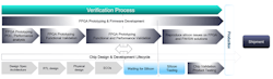
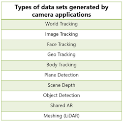
To test that all components connected to the SoC are working correctly, firmware and software development is essential for simulations before the silicon becomes available (Fig. 2).
If an issue is discovered during silicon testing, it’s vital to know whether the problem stems from the firmware (FW) or if it’s in the silicon. Firmware is used to verify silicon and works as the base layer for developers to create the software that serves as the backbone for users.
Testing external hardware components connected to the SoC also has to be completed before silicon is available, and this testing must use the physical design. Any issues must be fixed before tapeout. Performance monitoring and measurement of the SoC design with real hardware/data also needs to come before tapeout. FPGA prototyping of the SoC on a hardware platform provides the vehicle for all of these tests.
How the Process Works
To develop the firmware, the SoC partner with an experienced FPGA team will implement the design on an FPGA platform for functional testing.
There’s a limit to the number of functionalities and basic tests possible while the design is in progress. As a result, customers and partners must work together throughout the design process using the FPGA prototype to write the firmware, test the functions, perform the engineering change order (ECO), and retest to ensure that designs are done correctly and function well. Firmware is continuously developed as more features and functionalities are added.
The verification service accomplishes two major tasks simultaneously: Using the firmware to verify the functionalities of the design and ensuring the firmware is working correctly. The same FPGA prototype also allows customers to test other components of the product with the real design on a hardware FPGA prototyping platform. Because such activities happen in tandem with the physical design, they help accelerate the design process and eventual time-to- production.
Socionext’s FPGA and Design Capabilities
There are various commercially available prototyping platforms like HAPS, Protium, S2C, and so on. Socionext has established expertise in implementing large SoC designs on these various FPGA prototyping platforms, especially using Synopsys HAPS.
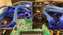
It’s able to implement an entire SoC on the FPGA platform (Fig. 3). Some companies have designs that have millions and billions of gates. Socionext has worked with designs that have 200-, 300-, and 500-million-gate designs.
That many gates can’t be put on a single FPGA for testing, so the company has implemented designs on boards with multiple FPGAs, with each board having up to four FPGAs along with the ability to stack boards. Sometimes four, five, and 10 FPGA boards are stacked together to put the entire design on the board to perform firmware testing.
In addition to implementing the design on multiple FPGAs, the design can be partitioned to fit on different FPGAs. An FPGA works a lot slower than an ASIC, at around 1- to 10-, 50-, 100-speed down version. However, the speed is sufficient for running tasks like taking videos and capturing network data, sending it to a processing interface to perform certain intermediary decisions delivered to the next chip, or patch.
SoCs are generally large and complex with various types of interfaces that need to be built and tested during this design phase (Fig. 4). Mobile-device interfaces may include Ethernet, SD card, MIPI, HDMI, and others, and these connectors need to be available on the FPGA platform for test verification. As they don’t all come from a single prototype platform, Socionext developed platform-compatible daughtercards for most standard interfaces and built custom cards that connect to these platforms, including daughtercards acting as interfaces.
Simultaneous development of the firmware on FPGA platform such as HAPS, used by Socionext and many others, makes it possible to provide the same data format to the customer. This means the customer’s FPGA boards can load the same data design database and then run the test from their side.
Such collaboration enables customers to concentrate on adding more layers or software on top of their designs while a company like Socionext builds on the initial one or two layers of software. Customers also can do this by using another partner’s base design with the first layer or firmware provided by Socionext for building software on top of it.
Mimicking Camera Data
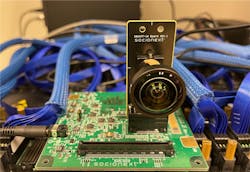
Not many FPGA boards on the market can run a camera using MIPI interface. There's an increasing demand from customers for this functionality, and special designs developed by Socionext addresss that issue. The boards mimic the camera data (Fig. 5) to generate test variance. Customers can feed that data to Socionext’s path to test the entire path.
In addition, daughtercards developed by the company use the MIPI chip and camera (Fig. 6) on top of the daughtercard so that customers can connect the camera using the MIPI chip to a HAPS board. Furthermore, an in-house test mechanism/generator can mimic the camera to run the tests, which can save customers’ time.
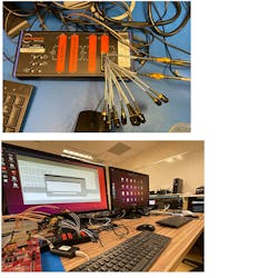
Socionext’s generator and analyzer devices can collect all kinds of data for the display and use that data to analyze the display on the video. Both types are available in the lab to run testing. This helps customers simultaneously generate multiple data sets and analytics. The single-device generator can verify numerous display channels using different kinds of cameras with the capability of sending a wide range of video or image file formats to the TV, phone, car, and other mobile devices.
On top of that, a protocol generator and an analyzer ensure each interface is compliant with protocols by global standards committees (Fig. 7).
About the Author
Vikas Gokhale
Senior Design Manager, Socionext America Inc.
Vikas Gokhale is a Sr. Design Manager at Socionext America. He possesses over 18 years of experience leading cross-functional, global teams in the development of complex system-on-chip (SoC) designs, from RTL to production silicon.
Comment About the Article
To join the conversation, and become an exclusive member of Electronic Design, create an account today!

Leaders relevant to this article: