Compact 16-nm FPGA Loads Up on Programmable Logic

Check out the other 2023 IDEA Award Nominees.
Lattice Semiconductor’s new Avant architecture is purpose-built to extend the company’s focus on high power efficiency, small form factors, and performance to mid-range FPGAs.
The company said the first family of FPGAs based on the new architecture, Avant-E, is designed for the purposes of real-time data processing and on-device AI inference, bringing twice the speed while expending 40% less power than existing chips for edge computing. The Avant series signals Lattice’s ambitions to become a more prominent player in areas such as communications, industrial, and automotive.
The Avant architecture marks a new chapter for the company. For the last several years, the focus has been on expanding its Nexus family of 28-nm FD-SOI FPGAs that puts power efficiency and small form factor front and center.
The new family puts the programmable chipmaker in direct competition with AMD’s Xilinx and Intel. Executives said the move will double its total market targeted by its products to approximately $6 billion.
What apparently sets Avant apart from the competition is that it’s designed from the ground up for the mid-tier of the market, which covers chips with 100,000 to 500,000 logic cells, and is suited for everything from industrial automation and robotics to automotive networking and software-defined radios. As the company explains, the Avant FPGAs are stripped of unnecessary features that can sap performance, power efficiency, area, and other properties that are high on the priority list for its customers, such as NI in test and measurement and Rockwell Automation in the industrial market.
“With Lattice Avant, we extend our low power leadership position in the FPGA industry and are poised to continue our rapid pace of innovation,” said CEO Jim Anderson.
Inside the Package
The new Avant family is expected to introduce major hardware innovations across the board, said Lattice.
While the most advanced chip in its Nexus lineup clocked in at 100,000 programmable logic blocks, Lattice is shooting higher with Avant. The FPGAs, which contain up to 500,000 logic units, operate at up to 350 MHz, bringing up to 5X more compute density into the fold over the Nexus architecture. Along with its advanced connectivity and AI hardware acceleration, these improvements put it a step ahead of alternatives in Intel’s Arria-5 and AMD’s Xilinx-designed Kintex-7 FPGA families.
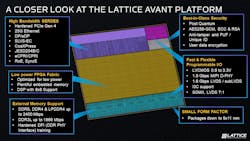
The company said it’s upgrading the Avant architecture to TSMC’s FinFET 16-nm node. That translates to a 50% performance boost for the programmable logic fabric at the heart of the FPGAs relative to Nexus, which was introduced in 2019. The process technology also keeps leakage current in check, reducing power compared to other devices in a similar class.
Avant features up to 28 SerDes that operate at up to 25 GB/s, which are configurable for a wide range of different connectivity protocols, providing upwards of 700 GB/s of bandwidth—10X more than the previous-generation chip.
The company is betting on its expertise in ultra-low-power FPGAs to extract as much performance as possible from the Avant chip while limiting power requirements. According to Lattice, Avant expends 2.5X less power and dissipates less heat than alternatives from AMD and Intel.
Less power consumption also allows for the use of smaller packaging: The flagship offering in the Avant-E family squeezes 500,000 logic units into a 15- × 13-mm package, while the chip containing 200,000 logic blocks fits into a 11- × 9-mm footprint, saving up to 6X more space on a circuit board than the competition.
In addition, Avant leverages Lattice’s existing software assets, including programming tools, reference designs, and software development kits (SDK) such as Lattice Radiant and Lattice Propel. The chips also support the company’s suite of application-specific solution stacks for embedded security, factory automation, and other areas introduced in recent years. Lattice said this would help its existing customers upgrade to Avant-based FPGAs faster and reduce time-to-market.
The Avant FPGAs come with a suite of IPs as well, including hardened logic to fit more performance in a smaller area plus “soft” configurations that impart more flexibility through the use of programmable logic blocks.
Furthermore, hardened controllers support up to 8x lanes of PCIe Gen 4 for ferrying data on and off the processor. Avant adds external memory interfaces for DDR4, DDR5, and LPDDR4 that run at up to 2.4 GB/s.
The FPGAs also feature fast, flexible programmable I/O that support everything from MIPI D-PHY to I3C.
Hardware Acceleration
Besides its power- and space-saving features, Avant can serve as a hardware accelerator for on-device AI inference.
The power of any FPGA stems from its flexibility. The programmable logic at the heart of the processors can be reconfigured at any time and out in the field—even after they’re embedded on a factory floor, in a data center, or under the hood of a car—to match them to specific workloads. This allows FPGAs to execute workloads, including machine learning, more efficiently than CPUs that tend to be more general-purpose in nature.
Lattice said Avant has the advantage of being more future-proof than custom-designed AI chips. The FGPAs can be remotely reprogrammed over time to match the latest advances in AI, instead of forcing customers to regularly buy replacement silicon.
Avant features up to 7,200 digital signal processors (DSPs) to efficiently handle AI workloads. The accelerators are tightly coupled with the programmable logic at the heart of the FPGA and a large amount (up to 36 MB) of embedded memory that enables larger machine-learning models to fit within the processor. The Avant chip also is equipped with up to 4 MB of on-chip RAM.
The flagship chip in the Avant-E family pumps out up to 5 trillion operations per second (TOPS) when running AI workloads at a 350-MHz clock rate. Lattice said that’s up to 30X more performance than its predecessor.
As a result, the Avant family of FPGAs is well-suited for use in factory equipment to detect faults further ahead of time, or in a robot to map its surroundings with faster real-time performance and higher image resolution, said the company.
For the purposes of embedded security, Avant has a hardened security engine that runs advanced cryptography (AES256-GCM), and it supports authentication (RSA4096) and error-correction code (ECC). There are also countermeasures to protect against physical attacks and tampering with the hardware.
The Avant-E chips are now available in sample quantities, with mass production apparently set for the first half of 2023. The company plans to roll out additional chips equipped with 200,000 and 300,000 logic blocks based on the Avant platform later in 2023.
Lattice said further additions to its Avant-based lineup will come to the market in the years ahead
About the Author

James Morra
Senior Editor
James Morra is the senior editor for Electronic Design, covering the semiconductor industry and new technology trends, with a focus on power electronics and power management. He also reports on the business behind electrical engineering, including the electronics supply chain. He joined Electronic Design in 2015 and is based in Chicago, Illinois.
Comment About the Article
To join the conversation, and become an exclusive member of Electronic Design, create an account today!

Leaders relevant to this article: