Massive Chiplet-Based FPGA Designed to Make More Chips
Check out our Design Automation Conference 2023 coverage. This article is also part of the TechXchange: Chiplets - Electronic Design Automation Insights.
What you’ll learn:
- What is the Versal Premium Series?
- What are super logic regions (SLRs)?
- Why the VP1902 is important to EDA chip emulation and verification.
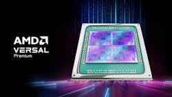
AMD’s (formally Xilinx) Versal Premium VP1902 adaptive System-on-Chip (SoC) is built around four super-logic-region (SLR) chiplets connected in a two-by-two layout via a silicon interposer (Fig. 1). A silicon interposer can be viewed as a printed circuit board but at the chip level. It’s able to provide thousands of connections between chiplets.
The chiplets are massive by themselves, but creating larger chiplets reduces the production yield because fewer rectangular chips can fit on a silicon disk. In addition, the number of potential defects ramp up. The size of the chiplet is optimized for the best production results.
The target application for this chip is emulation of new chips. Although a single VP1902 can emulate a sizable integrated circuit, multiple VP1902s on a board and multiple boards in a system are typically used to emulate today’s systems-on-chips (SoCs), which often have a million transistors.
The Versal Premium SoC contains 18.5 million logic cells. Each SLR has a quarter of that. The aggregate bandwidth of the SoC is 5.6 Tb/s—twice that of the earlier Virtex UltraScale+ VU19P FPGA SoC. The latest chips double the number of transceivers to 160, delivering an aggregate bandwidth of 12.2 Tb/s.
The SLRs are functionally identical chips with multiple North-South/East-West network-on-chip (NoC) subsystems for fast movement of data across a chip to connect different parts of the FPGA fabric (Fig. 2).
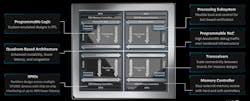
The fabric itself is conventional programmable logic, but NoCs can put data into a packet and move it through the NoC to another location on the chip or adjacent chips depending on the NoC and connections. NoCs are programmable, and this is typically handled by the FPGA design software.
Data can also be routed to and from the processor subsystem that consists of multiple Arm cores and the SerDes for off-chip communication. In addition, multiple DDR memory controllers on each SLR support off-chip storage. The LVDS15 XPIOs included on every SLR are designed for low-latency communication between chips.
Why FPGAs are Important for Chip Verification
These days, chips are never built from scratch. They’re verified and emulated many times before chips are actually made because the cost of a failed chip due to design or implementation errors can be massive. This is especially true for the more complex SoC chips being built with multiple processor cores, AI accelerators, GPUs, and more in a single device.
Over half the cost of a design is verification and validation. The term “shift-left” is currently used to indicate the movement of verification and validation further to the left in the design cycle.
Software emulation is always possible, but the speed is limited by the underlying hardware and software. Hardware emulation utilizes FPGAs like the VP1902 to evaluate a chip design more quickly than software emulation. Still, multiple VP1902s are usually needed to emulate a very large chip requiring more sophisticated design and synthesis tools (Fig. 3).
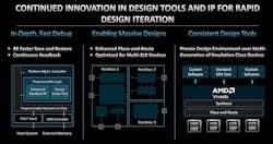
AMD’s Vivado is the software utilized to layout an FPGA implementation of a logic design. The challenge for the software is to optimize the use of the NoCs and the silicon interposer connections available in a Versal Premium chip, which is no easy feat and one that’s essentially hidden from the developer.
Debugging the emulated chips is one thing; debugging the emulation is another. The VP1902 includes improvements that provide more insight and accelerate the extraction of data within a configuration for debugging purposes. The support can perform full save-and-restore operation via enhanced readback IP and data can be streamed through PCI Express. The system supports continuous readback with selective scan-chain register readback.
Emulation and verification aren’t the only applications for the VP1902, although these applications will suck up a sizable chunk of the devices when they become available. Large, high-speed FPGAs are used in high-performance applications such as military radar and artificial-intelligence applications where soft logic provides an advantage for performance and updates.
Check out more of our Design Automation Conference 2023 coverage and more articles in the TechXchange: Chiplets - Electronic Design Automation Insights.
About the Author

William G. Wong
Senior Content Director - Electronic Design and Microwaves & RF
I am Editor of Electronic Design focusing on embedded, software, and systems. As Senior Content Director, I also manage Microwaves & RF and I work with a great team of editors to provide engineers, programmers, developers and technical managers with interesting and useful articles and videos on a regular basis. Check out our free newsletters to see the latest content.
You can send press releases for new products for possible coverage on the website. I am also interested in receiving contributed articles for publishing on our website. Use our template and send to me along with a signed release form.
Check out my blog, AltEmbedded on Electronic Design, as well as his latest articles on this site that are listed below.
You can visit my social media via these links:
- AltEmbedded on Electronic Design
- Bill Wong on Facebook
- @AltEmbedded on Twitter
- Bill Wong on LinkedIn
I earned a Bachelor of Electrical Engineering at the Georgia Institute of Technology and a Masters in Computer Science from Rutgers University. I still do a bit of programming using everything from C and C++ to Rust and Ada/SPARK. I do a bit of PHP programming for Drupal websites. I have posted a few Drupal modules.
I still get a hand on software and electronic hardware. Some of this can be found on our Kit Close-Up video series. You can also see me on many of our TechXchange Talk videos. I am interested in a range of projects from robotics to artificial intelligence.
Comment About the Article
To join the conversation, and become an exclusive member of Electronic Design, create an account today!

Leaders relevant to this article: